Electronics Design
Introduction
We were tasked to redraw, design and produce a PCB on our own. Specifically, a hello-world board using another ATtiny85. The program used to make the PCB design was Autodesk EAGLE. All we were given was the schematic, a reference picture of the traces, a picture of the final product and additional assignments such as adding an LED with a current limiting resistor and a switch.
Using EAGLE
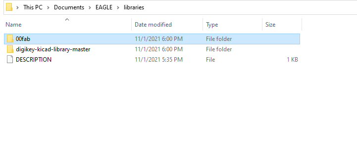
Immediately after downloading EAGLE, the first thing to do was to add the Fablab EAGLE Library, containing the components we will use for this module. To add the library, first download and unzip the folder. Then navigate to Documents -> EAGLE -> Libraries, and move the unzipped folder into this libraries folder. As EAGLE sorts libraries alphabetically, I made it easier to find by adding '00' to the front of the library name.
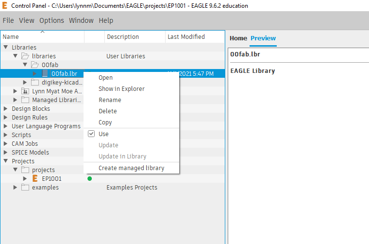
Once the library is added, I activated the library by opening up EAGLE, and on its control board expand libraries, expand the folder, right-click the .lbr file and click use.
Now that the set up is done, it is time to move on to the assignment.
Assignment
We had a choice of 3 Echo Hello Boards using different ATTiny Microcontrollers. I chose to do the board that used an ATTiny85.
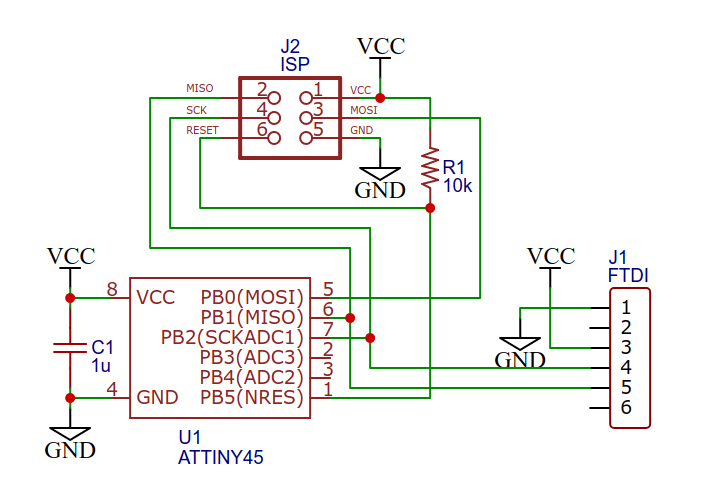
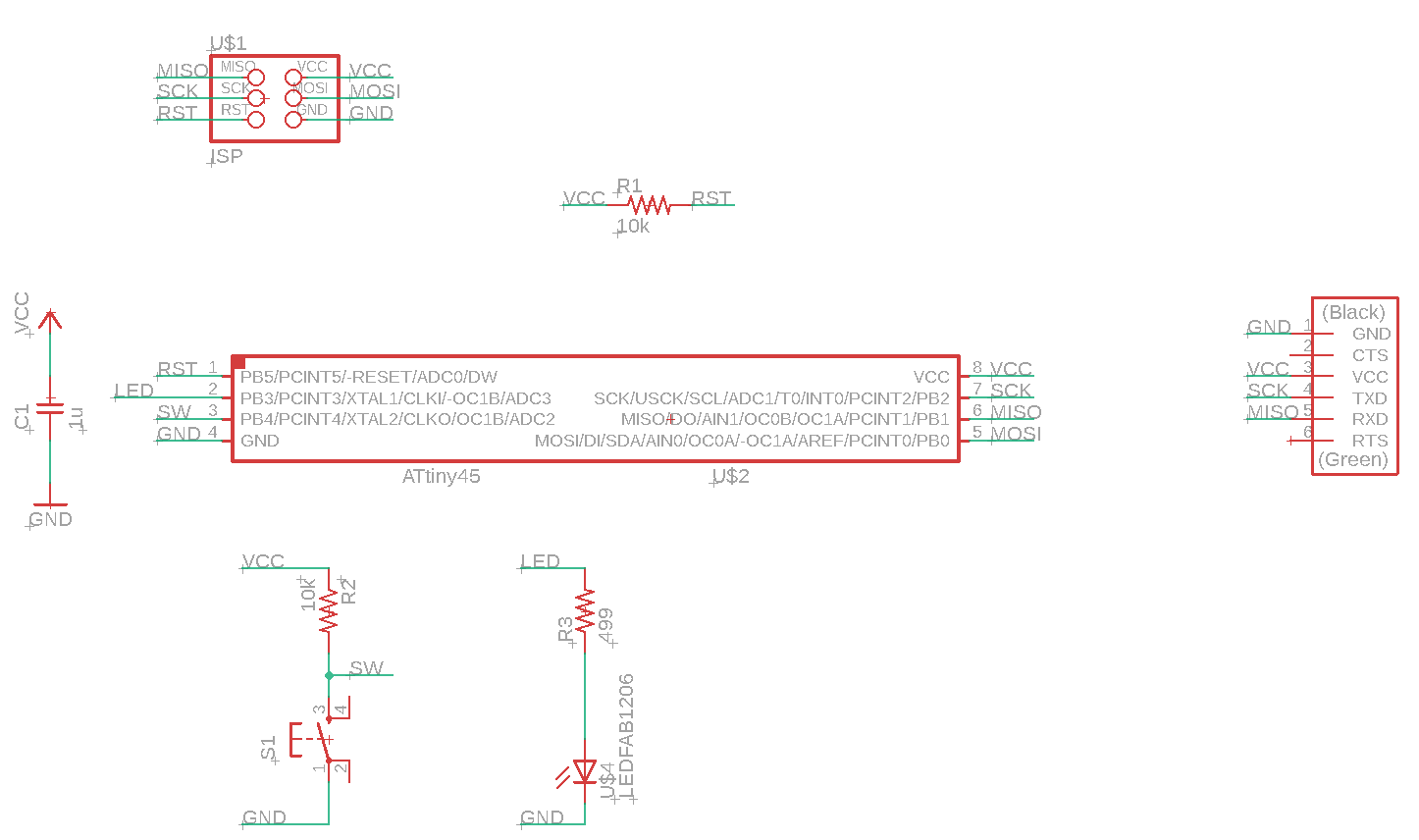
I followed the following schematic for the project.
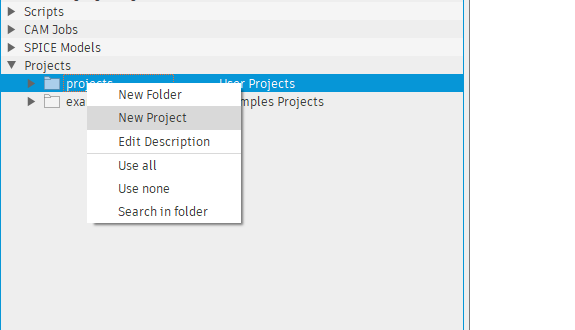
First, a new project is made by right-clicking the "projects" folder under "Projects" and clicking New Project. The project is just named ep1001.
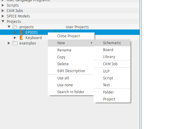
A new schematic is made in the folder by right-clicking the project and clicking New -> Schematic. The schematic is just named HelloBoard.
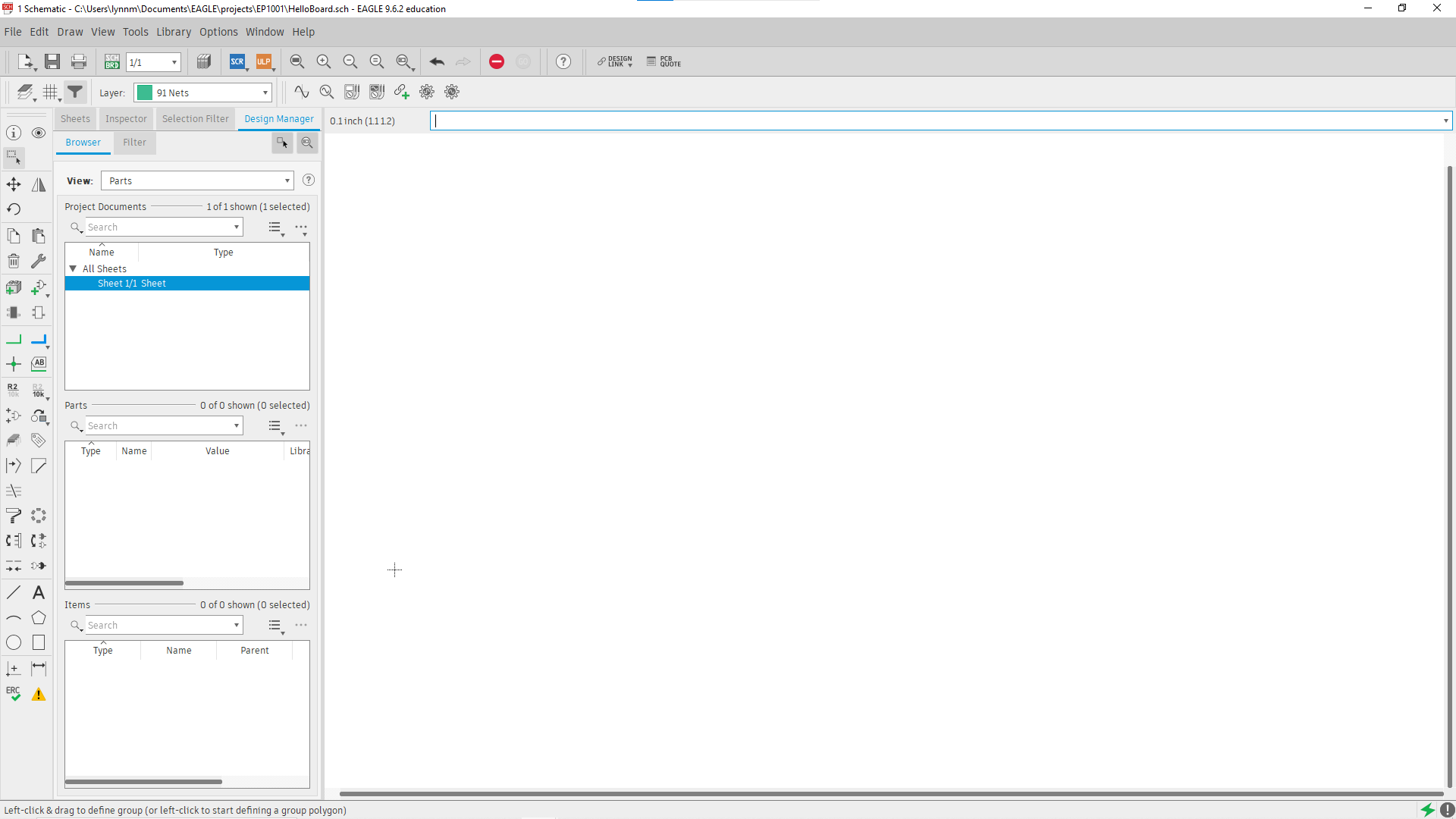
I was then taken to the schematics page.
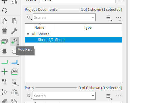
Now, we can start adding the parts needed for our pcb. To add a part, there is simply an "Add Part" button on the left navbar, shown in the picture below.
Once clicked, a window with a large library would be opened. If I was missing some libraries, I would have to go back to Eagle Control Panel, right-click on library and click "use all". In the window, I browsed for the part I need, or used the search function.
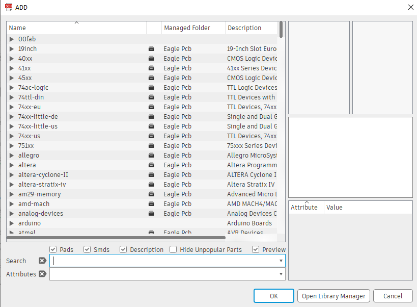
To search for a part, just part of the name will do, however, the search item needs to have a * at the front and back of the word. For example, I wanted to add the ATTiny85 IC into the schematic. I can either spend a long time looking for it in the different libraries, or I can just search for "*attiny45*" in the search bar.
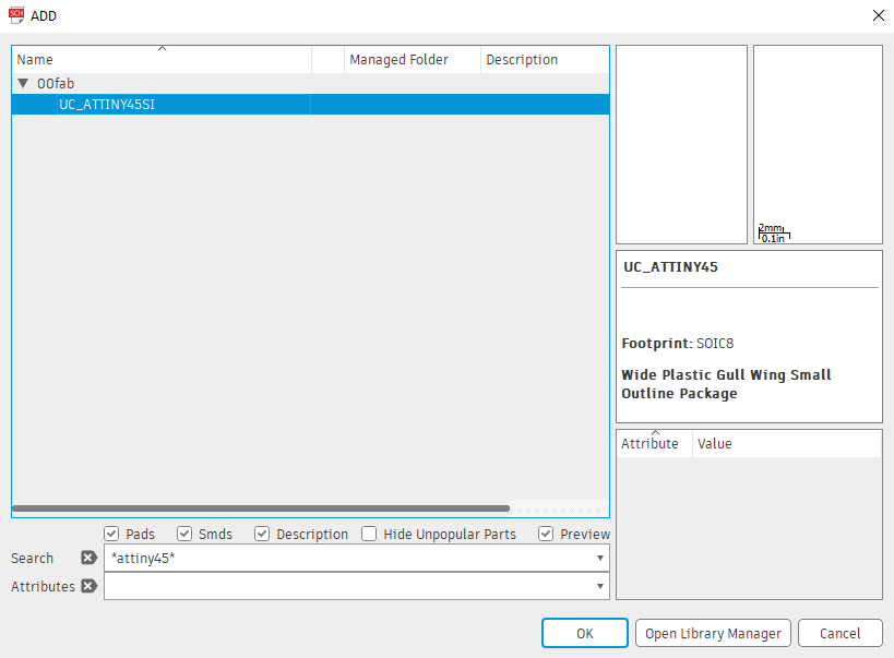
With no options for different packages, I chose the part and placed it into the schematic.
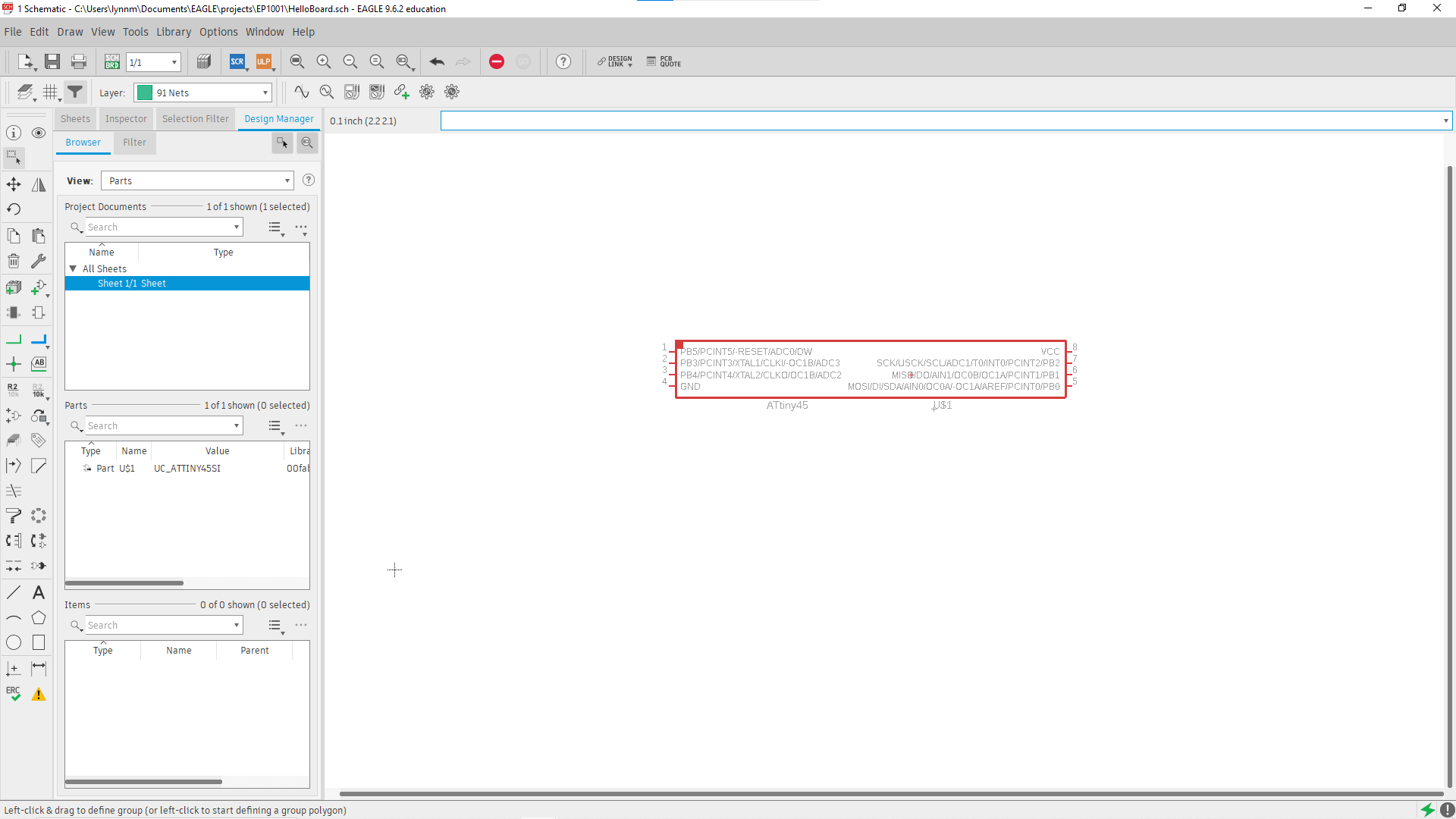
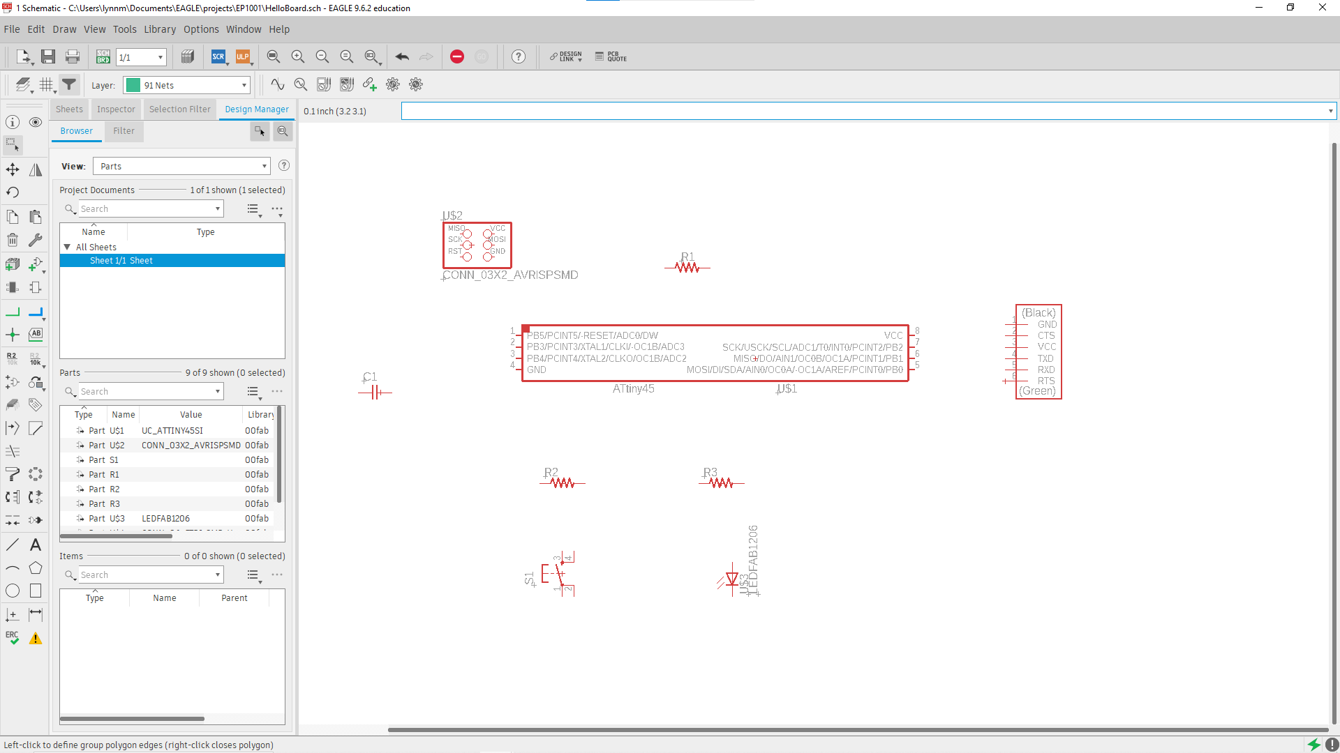
Using this method, the rest of the components were added to the schematic. From the example schematic given, I added
- ATtiny45 x 1
- 2x3 pin ISP header x 1
- 6 pin FTDI header x 1
- 10kΩ resistor x 1
- 1uF capacitor x 1
In addition to these components, the assignment also calls for adding a button and an LED (with a current limiting resistor). For this part, 4 more components were added.
- 10k Resistor x 1
- 499 Resistor x 1
- Red LED x 1
- 6mm Tactile Switch x 1
With all the components, the window should now look like this.
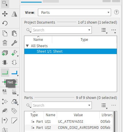
I planned to use R2, a 10k resistor as a pullup resistor for the switch, and R3, a 499 resistor as the current limiting resistor for the LED. At first, to make the connections I just connected them directly to each other using the "net" tool, found in the left navbar, shown in the picture below.
After wiring to the diagram plus adding the switch and LED, this is what I ended up with.
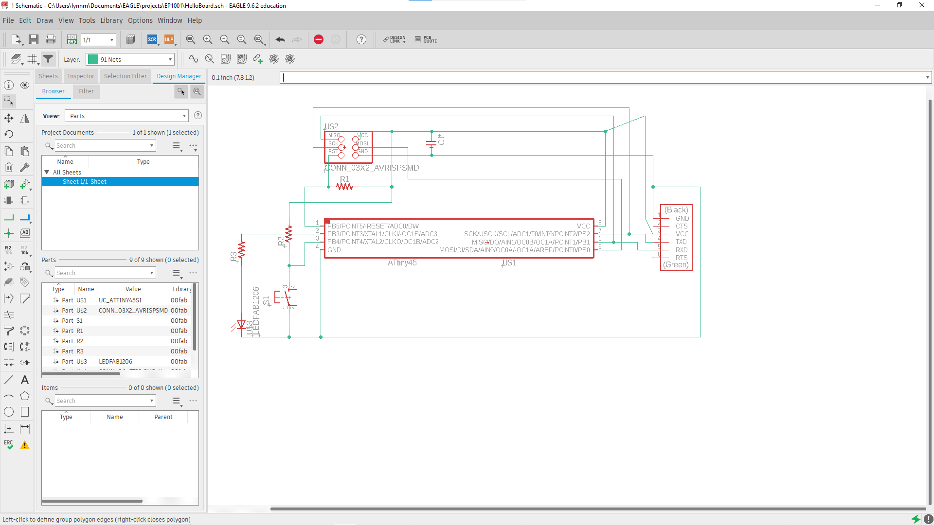
Although the connections might work, the whole schematic looked really ugly and it was hard to modify or add new parts if needed, as the wires were too complicated. that was when I found out about the "Name" tool.
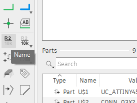
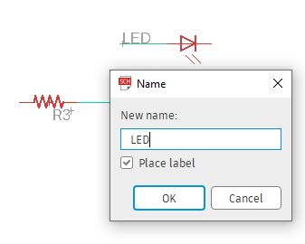
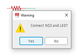
Names allows me to connect components together without the need for a net to be placed between them. The part just has to have a small net line coming out of it. The nets that I want to connected are then Named the same, in this case LED. Once both have been named, the program would treat it as if theres a net between them. When naming the second part, a warning will show up asking if I meant to connect the 2 nets.
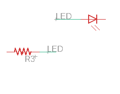
I did this to the entire schematic as it made it easier to navigate and modify if need be. After all the connections were made, here is my final schematic of the Hello Board. At this point, I also took time to add values to the resistors and capacitors. The value tool is found right next to the name tool.
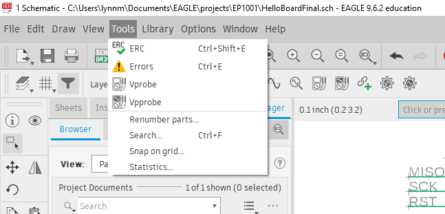
Before moving onto the physical tracing of the board, an Electrical Rule Check, ERC is done. This checks for any errors made while wiring. Nothing popped up after the ERC and I was good to go. The ERC is found under tools in the top navbar.
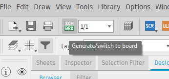
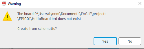
Now it is time to make the physical traces. To start, a new board has to be generated by clicking the green "Generate/switch to board" button in the top navbar. A prompt appeared asking if I would want to create a new board from schematic, I just click yes and move on.
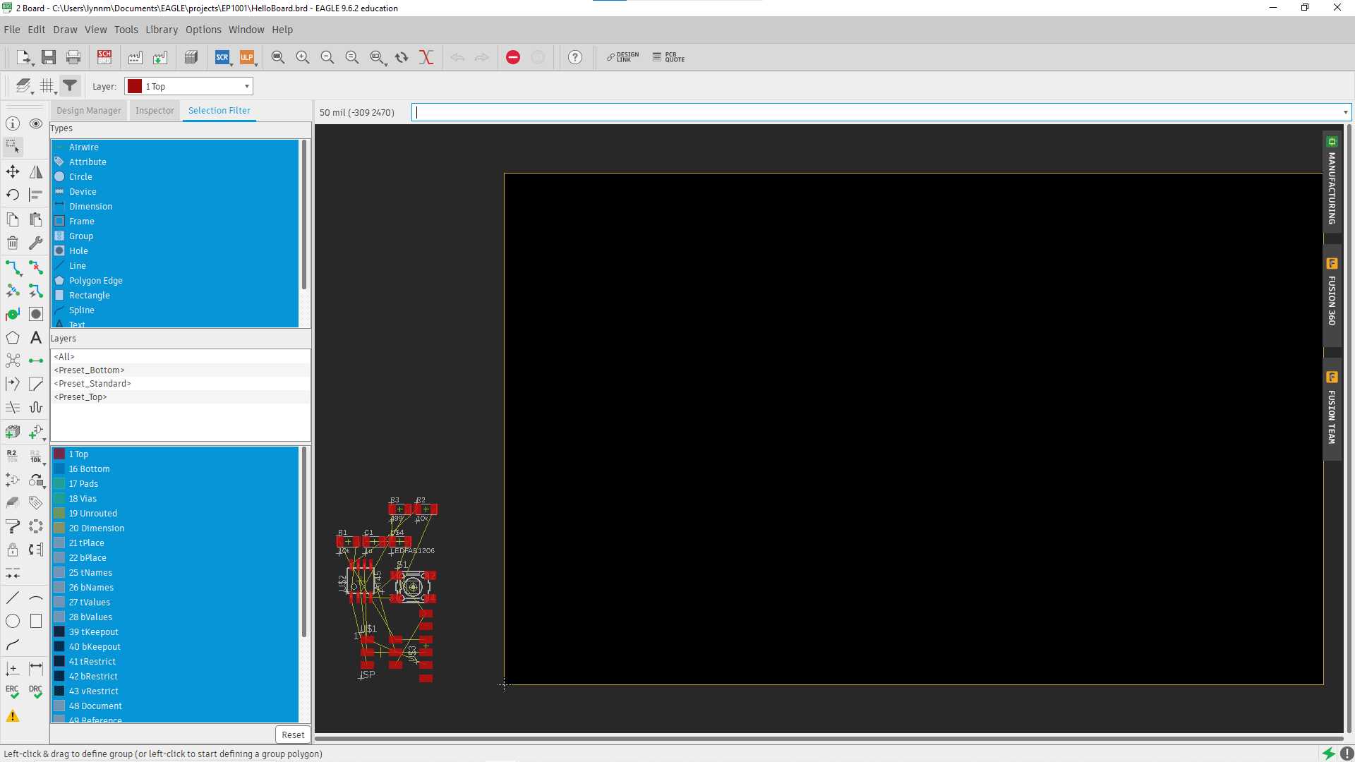
When the new board was made, I was brought to a new window with different navbars. In the workspace, there is a yellow rectangle, and all the components placed earlier should be in the bottom right.
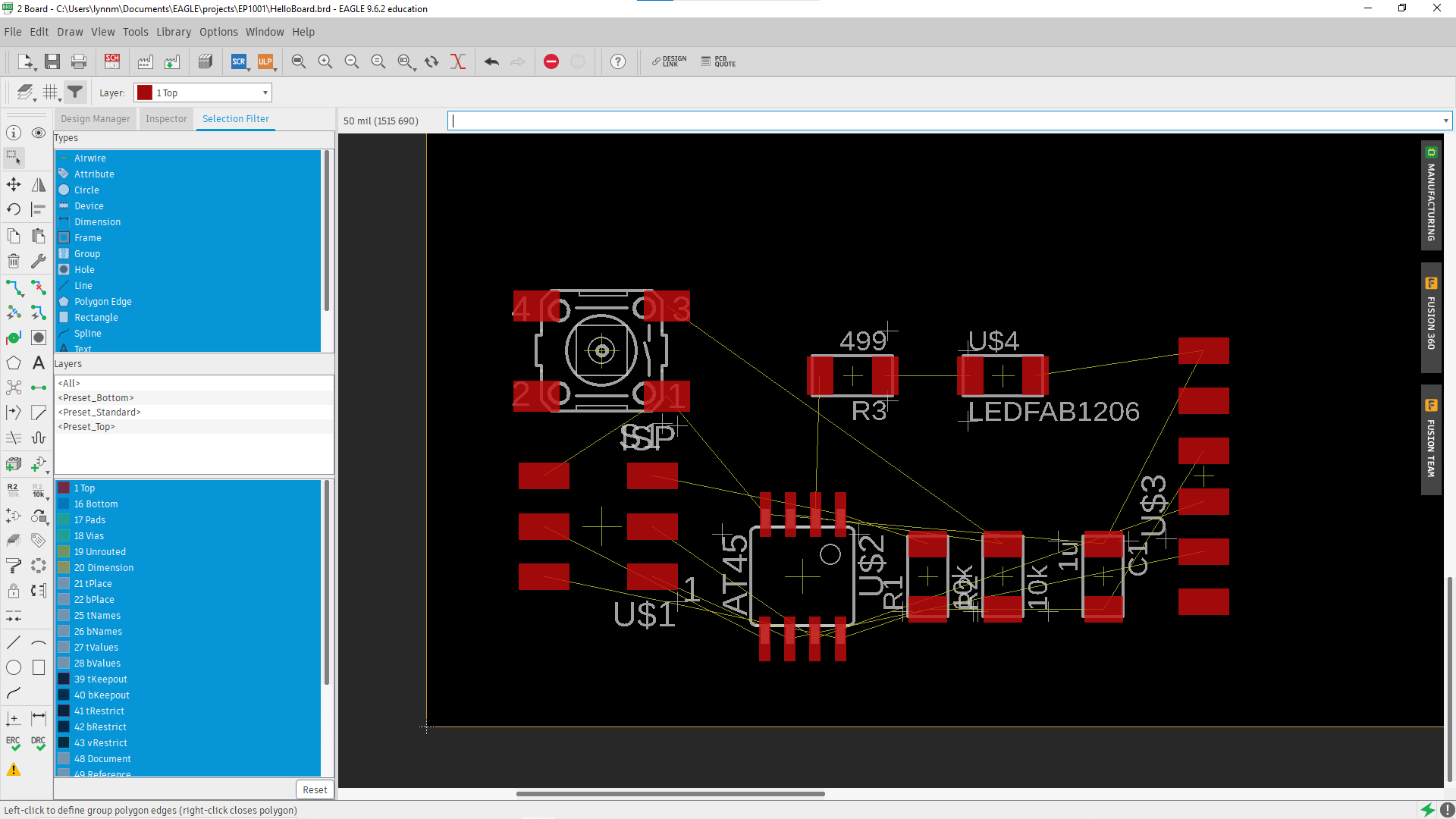
Designing a board from scratch is quite difficult with no experience, so for the main components, I followed the example board that was given to us. Using the move and rotate tools, I placed the components generally where they should be on the example board. From there, I made some changed to accomodate the switch, LED and 2 more resistors. Below is the first attemplt at placement of the components.
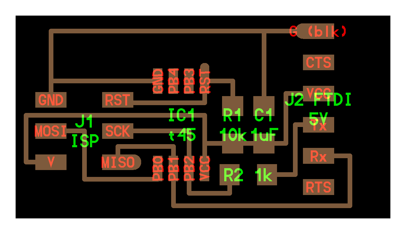
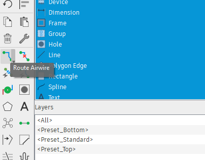
After this was running traces through the board. There is an autorouting feature, however I wanted to try manual routing first. The "route airwire" tool is what I used and can be found in the left navbar. After clicking the route airwire button, at the top there are some settings. The settings that were changed are the wire bend (First option, determines how the wire bends) to 90 degree bends and the thickness of the wire to be 16 as recommended by my lecturer Mr Steven Chew. The base unit for Eagle is mil, or 1/1000 of an inch. So the wire thickness was set to 16mil, or roughly 0.4mm.

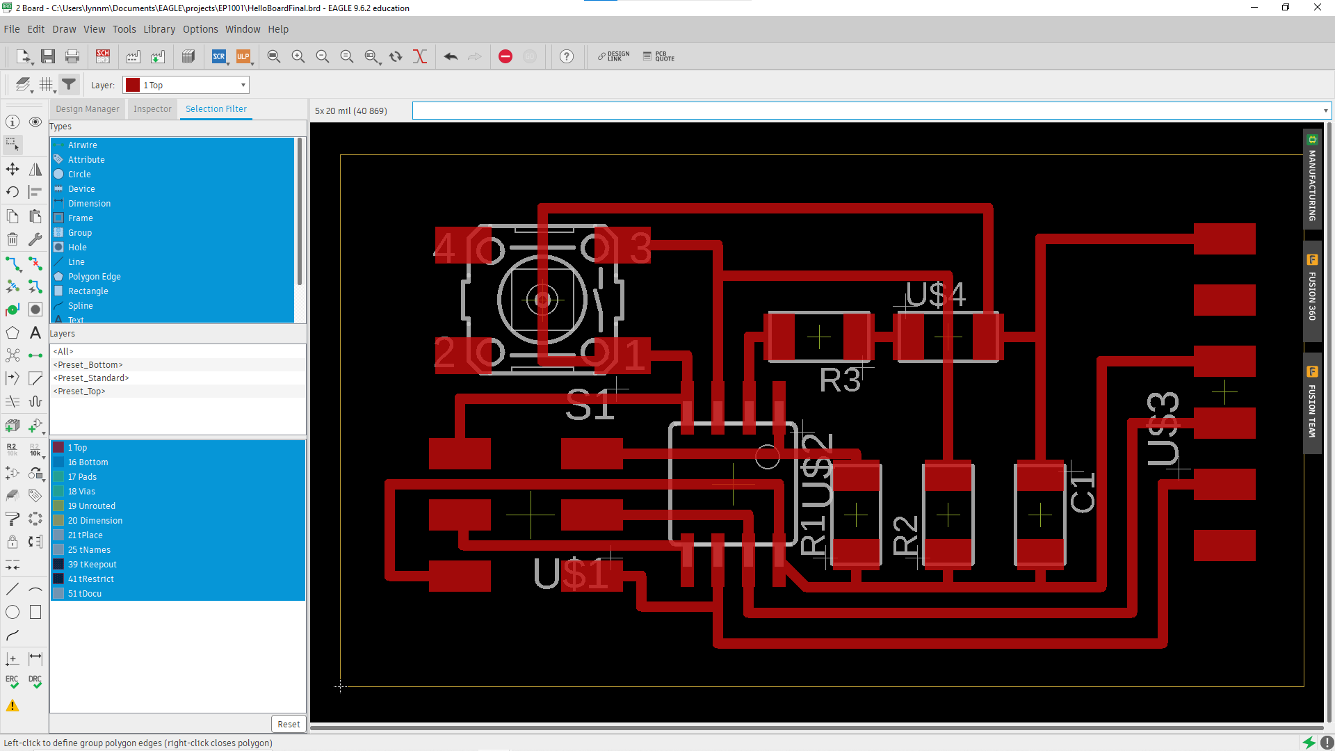
After changing the settings, the traces that need to be connected are just airwired together. Like earlier, I followed the example board first for the main components, then tweaked it a bit to fit my other added parts. After much trial and error, moving things around and such, this was what I ended up with. I also brought in the yellow border of the workspace just by clicking and dragging the yellow lines.
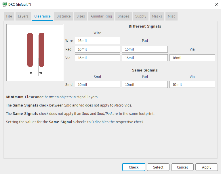
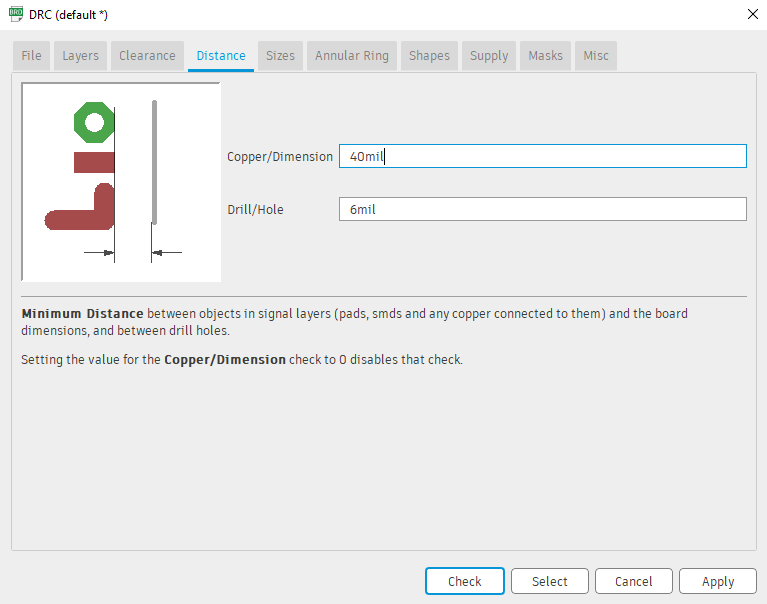
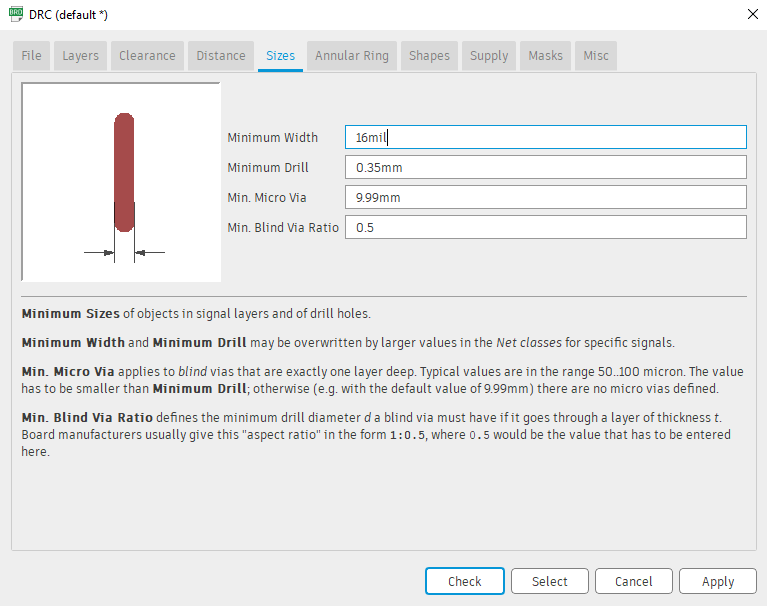
During the process of routing traces, I was constantly checking the Design Rule Check (DRC), which can be found under tools in the top navbar just like the ERC. The following settings in the DRC were changed from default. I clicked check and nothing major appeared, so I was good to go.
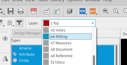
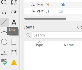
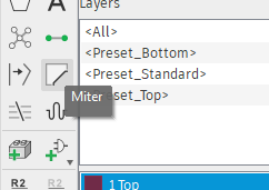
Last was the outline of the board. I first went to the milling layer. Layers can be found in the top navbar. A simple rectangle was drawn using the Line tool found at the bottom of the left navbar, then the corners were rounded using miter tool, found in the middle of the left navbar. Thickness and radius/type of miter is changed at the top navbar, just like trace width. All this was done just to make the board smaller and easier to manage.
After all that was done, this was the final board with outline.
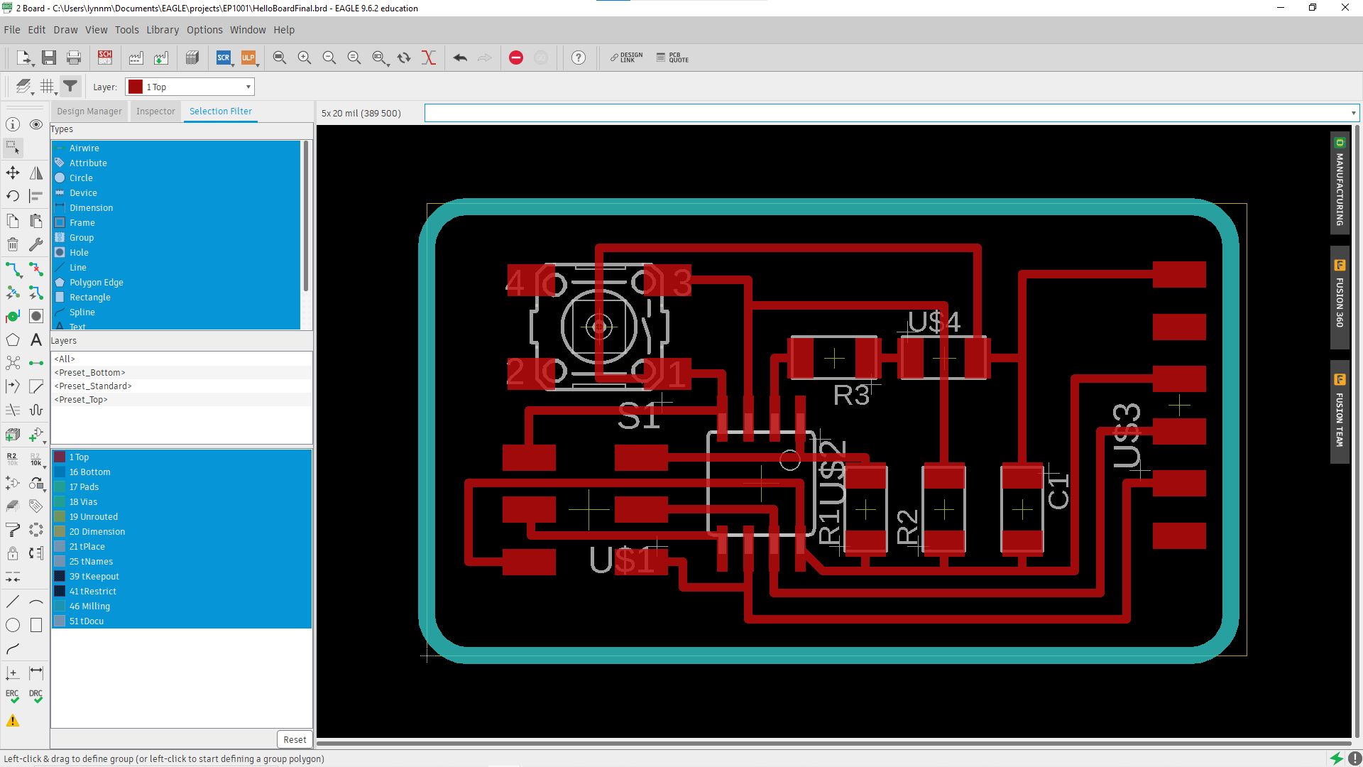
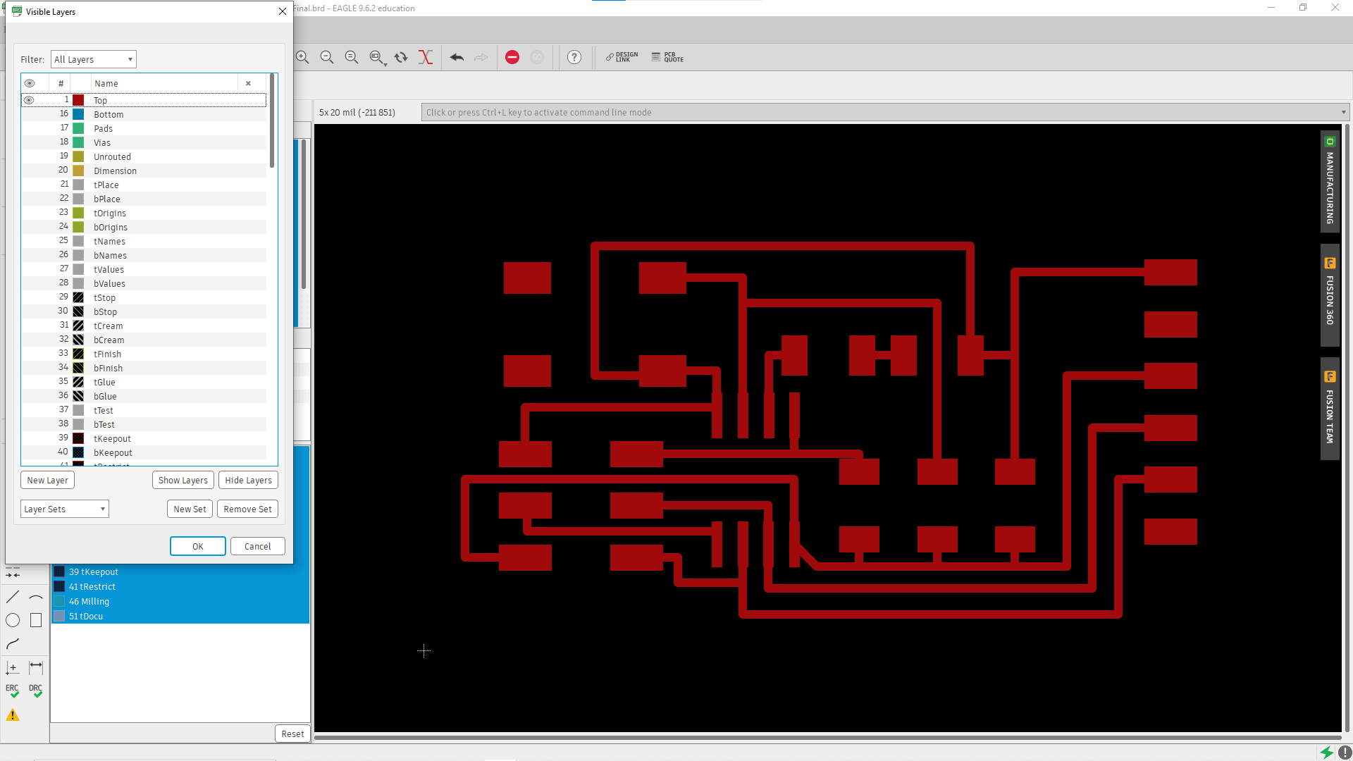
The next step is to export the traces and outline as png so that mods can generate the gcode. First, only the layer that is being exported is shown at one time, so we need to go into the layer settings in the top left.

Once the layers menu is opened, just hide all layers except the top layer, as we only want the top traces.
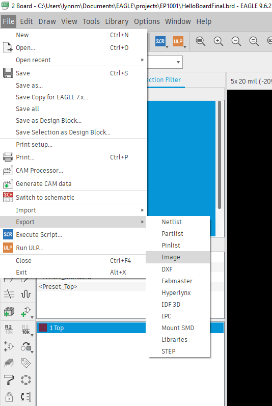
To export as PNG, go to file -> Export -> Image. In the export menu, choose where to save the image, click monochrome and increase the DPI of the image. In my case, it went from 150dpi to 1500. This provides a clearer image for mods to generate a more accurate gcode.

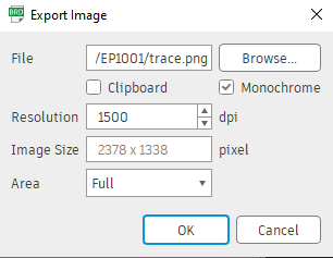
I did the same steps to export the milling layer which contains the outline. Afterwards, I ended up with 2 pngs, one for traces and one for the outline.
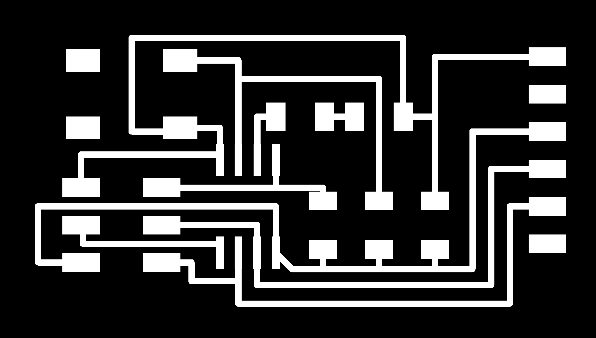
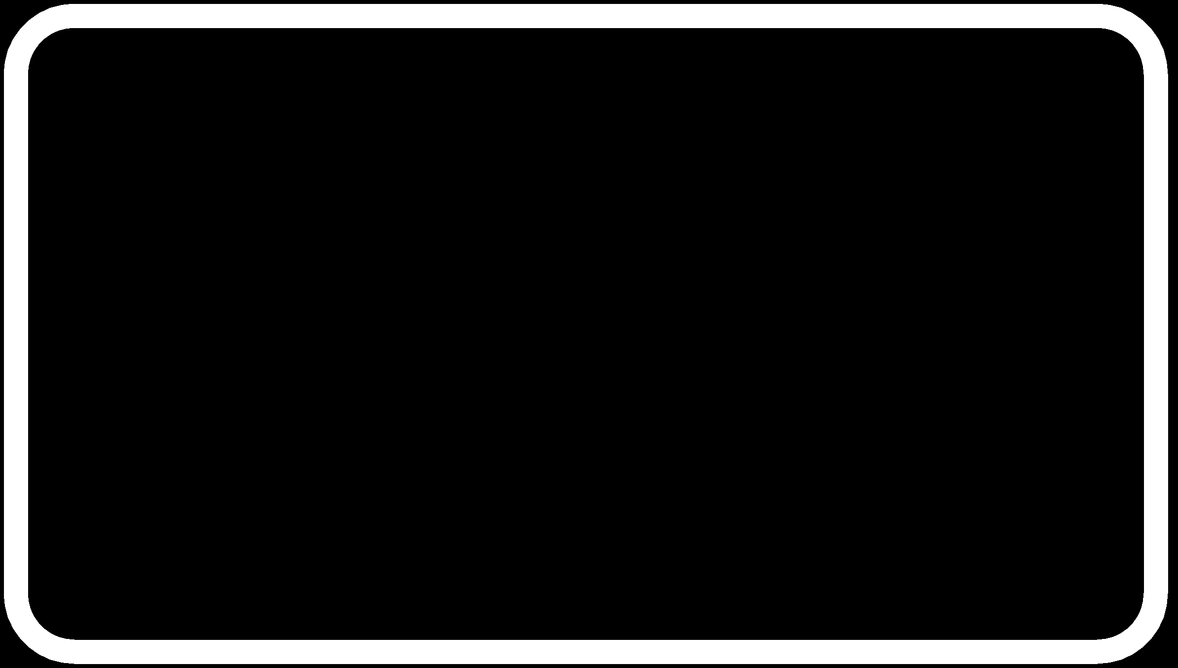
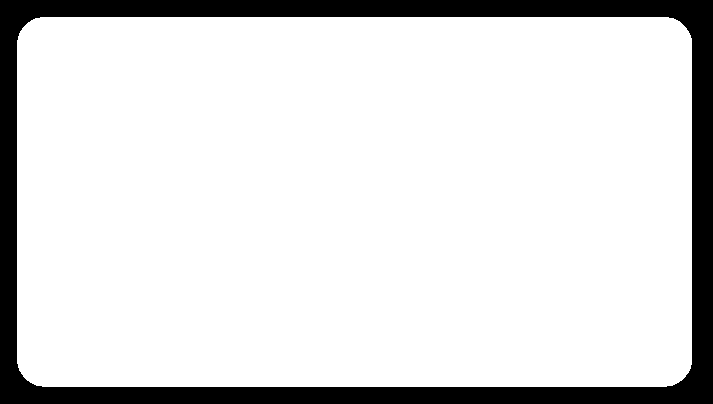
However, the traces for the outline is sort of wrong. Mods will only look at the boundary between white and black and treat it as an outline. As the current outline png is a white rectangle, the gcode will generate 2 passes for the outline, and I didn't want that. So, I imported the image into gimp, inverted the colors and filled the inside with white. This way, the gcode will only generate 1 pass on the outline. Here is the final outline PNG.
The gcode was generated using mods and the same settings as stated in electronics production. After a half hour of milling, what I had was a board which I can start stuffing.
Before
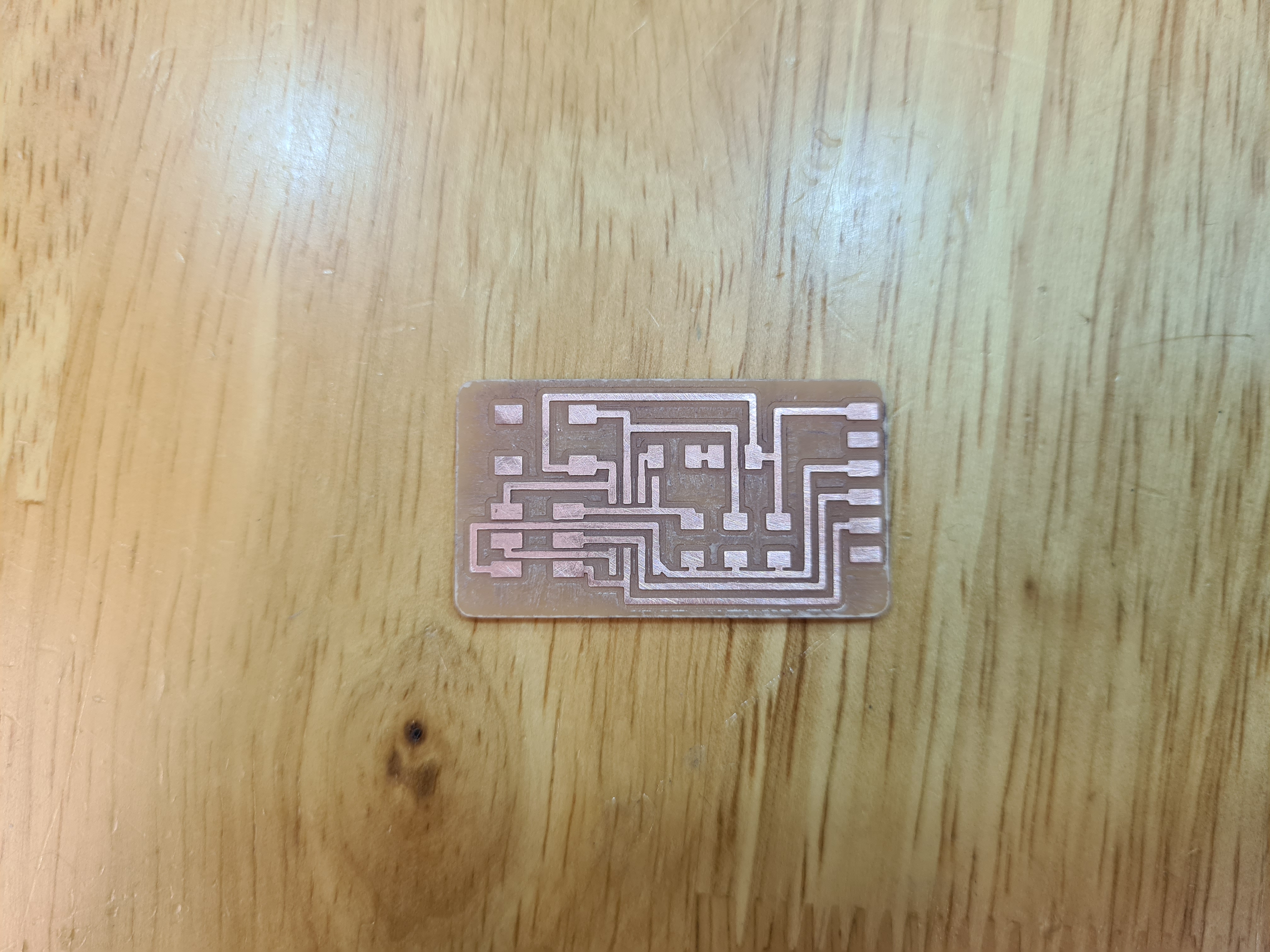
After
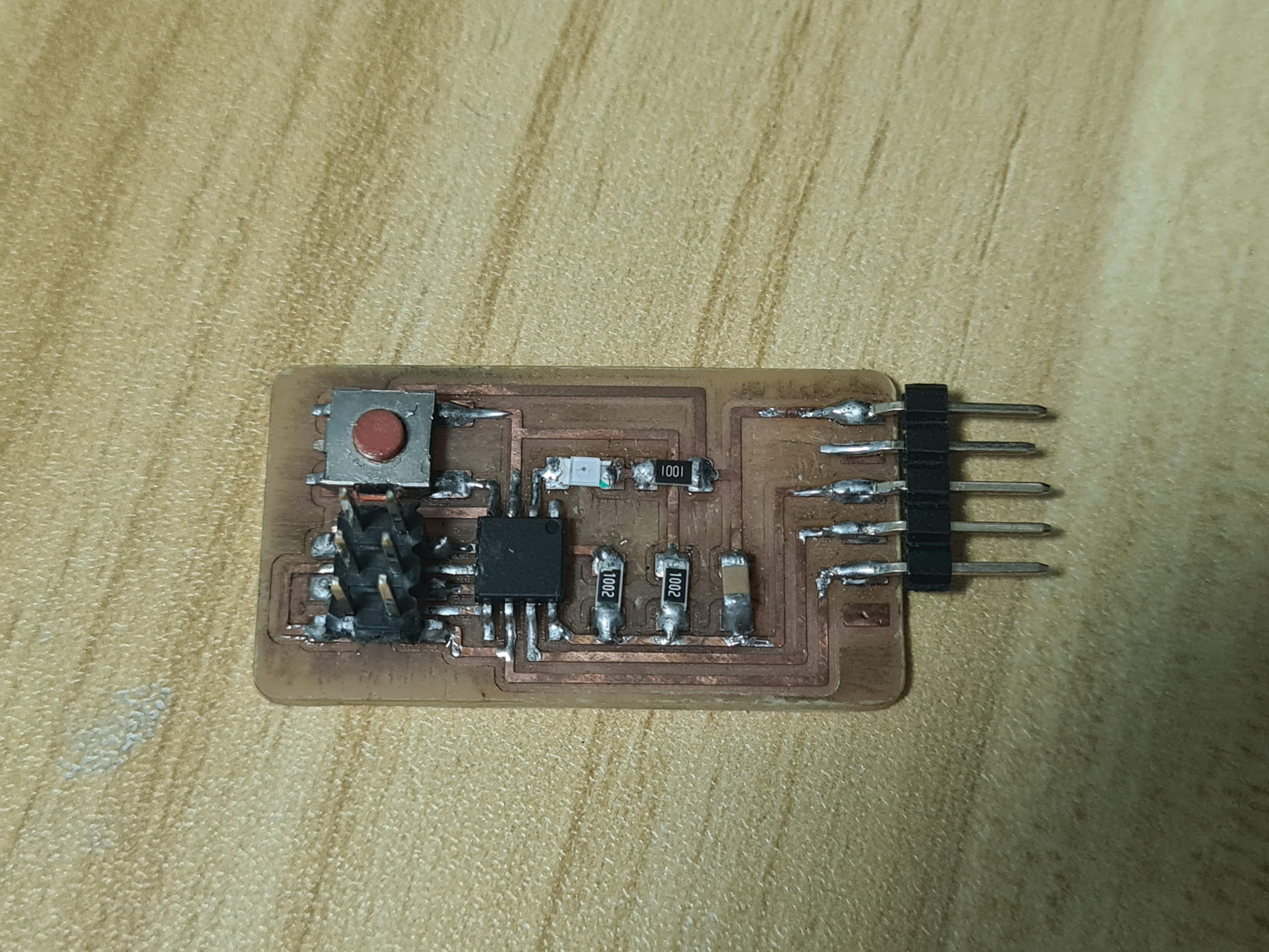
After all the components were stuffed, I used a multimeter to check to see if all the connections are correct and if there were any shorts. Luckily there weren't any so my Hello Board was good to go. I did make some mistakes during the design process though. One of them is the fact that the FTDI header was hanging off the board.
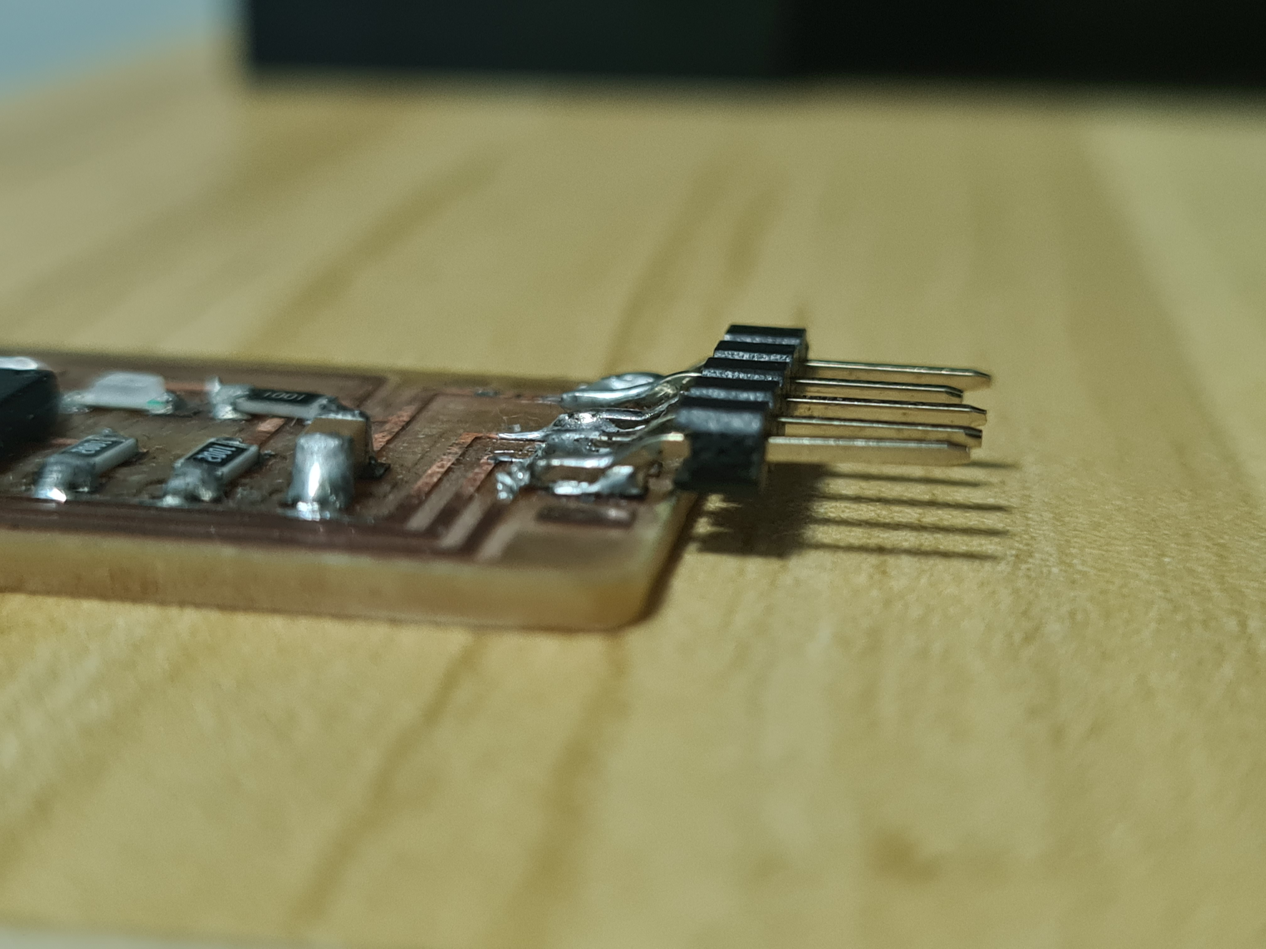
Because the FTDI is hanging by the trace, if I am not careful with how I handle it, I might rip the traces right off. The only fix for this would be to extend the outline past the FTDI traces in Eagle, remill and stuff another board, however I did not have time for that so I just stuck with this. In the future. I will keep this in mind when designing new pcbs. And with that, my Hello Board was done. The next time I will use this is during embedded programming.
Files
Hello Board SchematicHello Board Layout