Final Project
Disclaimer
I don't know exactly why or how the code of my project works. 2 of my friends tried to replicate a similar project but both did not manage to get theirs working. Procede with caution when attempting to replicate my project.
Table of contents
- Requirements
- Ideation
- Bill of Materials and files
- PCB Design
- PCB Manufacturing
- Stuffing the PCB
- Testing the PCB
- Case Design and Manufacturing
- Integration
- Coding
- Final Results
- Final Thoughts
Requirements
This is an individual capstone project that integrates the range of technologies covered in this module.
The final project must include:
- 2D and/or 3D designed part(s)
- subtractive manufacturing (i.e. cnc) part
- may include:
- molded or cast part(s)
- 3d printed part(s)
- laser cut part(s)
- an embedded microntroller that you designed & fabricated
- input and/or output device(s) that interacts with the user
- embedded program
Ideation
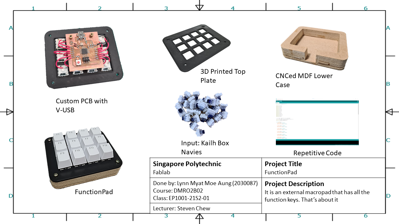
For my final project in this module, I wanted to make a keypad with function keys for the laptop. My current keyboard that I am using is a small form factor keyboard, as a result it is lacking the function row. During class work, I tend to use the function keys a lot in other programs, and it is slowly starting to become a hassle to press function with my left hand while doing work. Moreover, I wanted to experiment with virtual-usb for the atmega328. So, I decided to make a 12 key function pad, with F1-F12 as its binds. I also had some cherry mx style mechanical keyboard switches lying around so I wanted to incorporate it into my project.
Bill of materials and source files
PCB Components
- Atmega328 x 1
- 49 ohm resistor x2 (replacing the 68 ohm resistors in the schematic)
- 10k ohm resistor x 1
- 15k ohm resistor x 1
- Female mini usb x 1
- 1N4148 Diodes x 2
- 16 MHz resonator x1
- 6mm switch x 1
- 10uF capacitor x 1
- 0.1uF capacitor x 1
Remaining hardware
- 15mm MDF sheet
- Kailh Box Navies (or any cherry MX Style switch) x 12
- Keycaps (F1-F12, or any that you fancy) x 12
- Mini USB cable
Files
Final Project Arduino codeCase F3d files (contains all 3 parts as bodies)
PCB Schematic
PCB Layout
Technologies Used
- Large Format CNC
- 3D Printing
- PCB milling
PCB Design
To get started on the PCB design, I first referenced an example of a v-usb keyboard by OBDEV found here. The zip file given contains a schematic that I referenced.
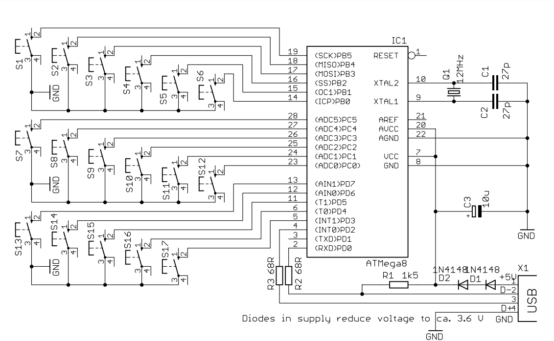
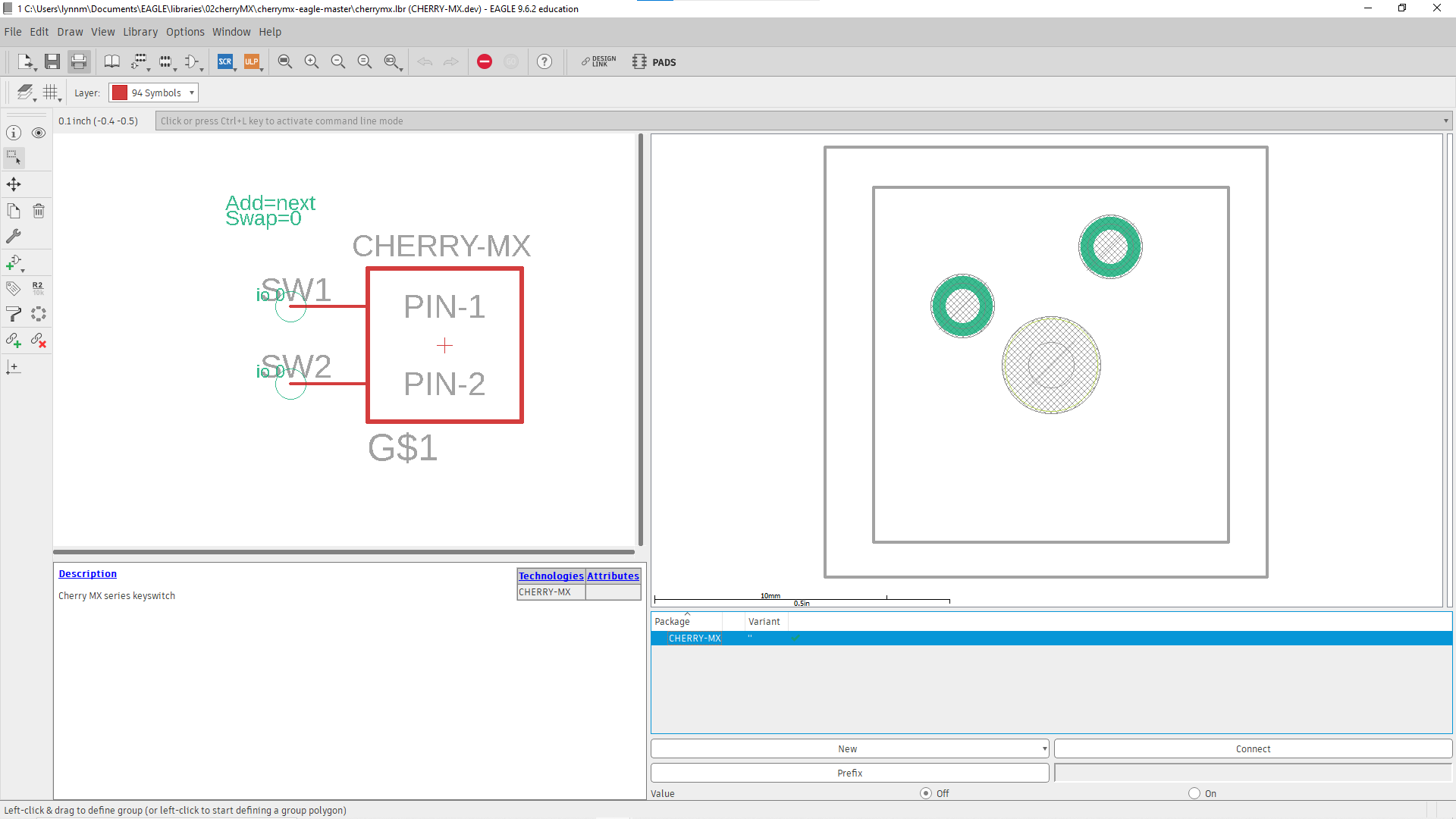
I referenced the connections of the oscillator, decoupling capacitor, and most importantly the connections for the USB. Originally, I wanted to make one large PCB with the cherry mx switch profile. The footprint is a modified version of a library from this github repository. I modified it to not have the stabalising pins on the sides, and to include the footprint for a keycap, as it would make the layout of the switches easier.
However, at this point I got a bit nervous about the size of the PCB. Each keycap had a length and width of 18mm, and with space between the keycaps, space for all the other components, and routing all the traces on a single layer, the PCB required would be bigger than the small rectangles we got. While the fablab did have larger PCBs available, I felt that I would mess up quite often during the manufacturing. As such, I opted for a different approach.
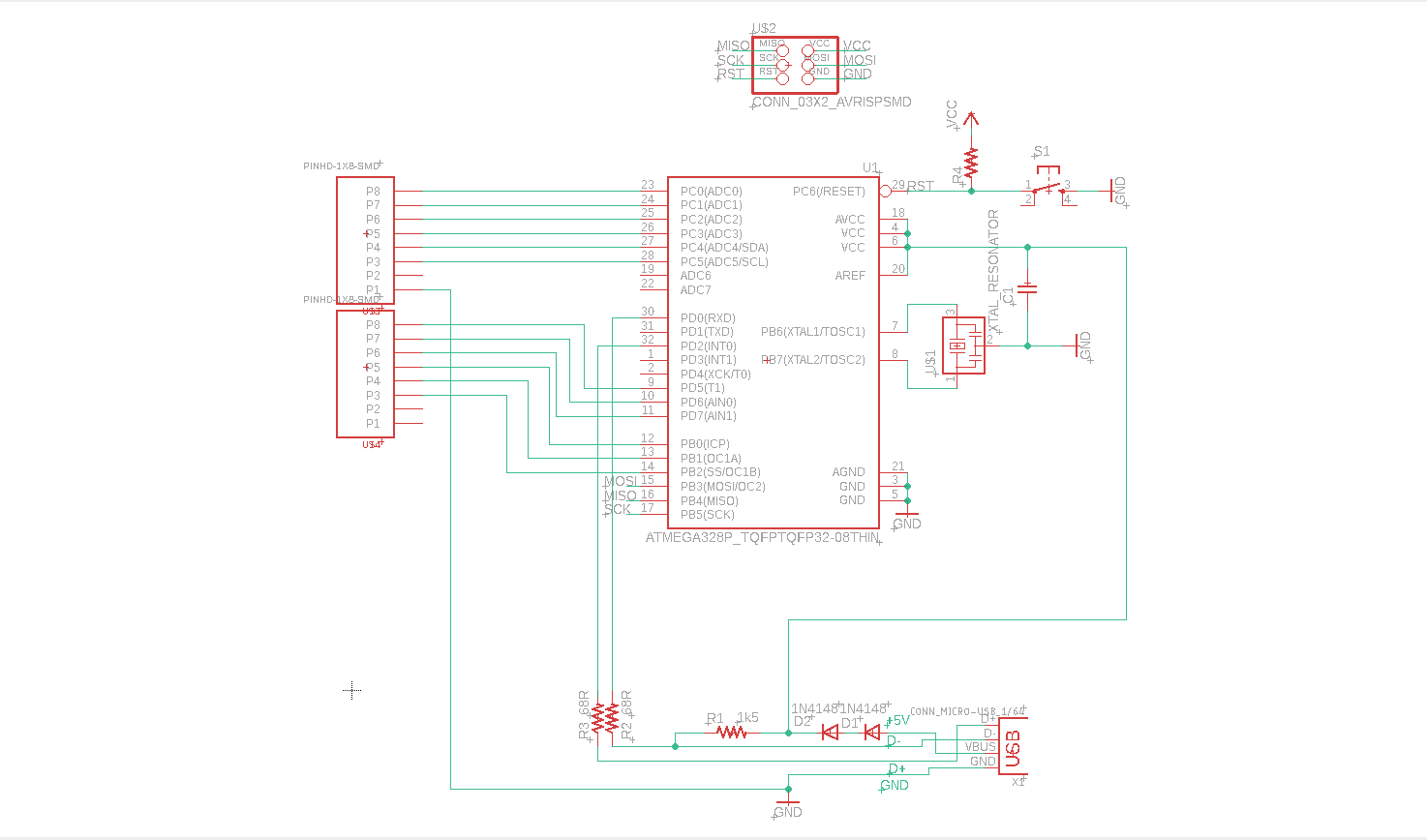
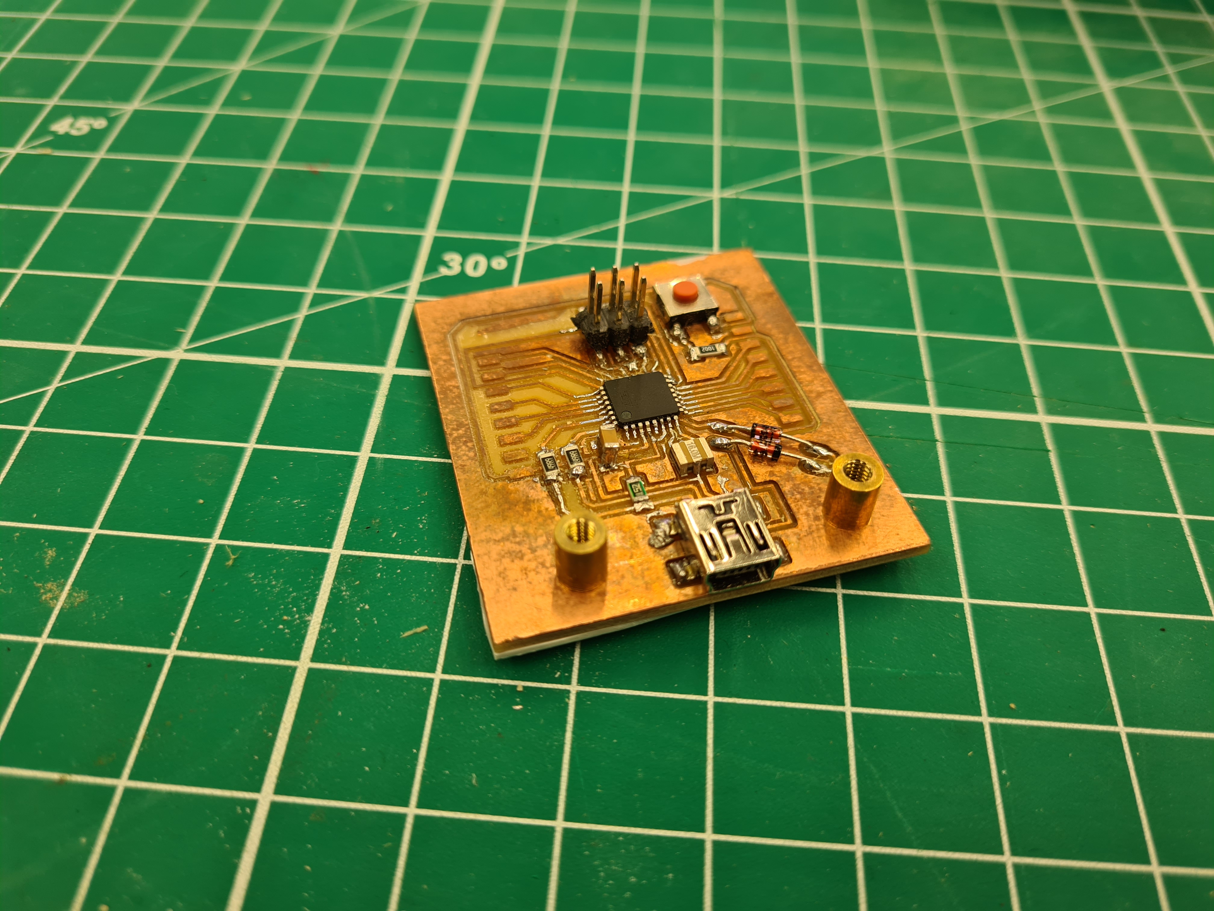
This may be a cop out, but my final PCB idea is to use the pads for an 8x1 header as the outputs to the switches, and solder wires directly on. I know that wires are frowned upon, but at this point I felt it was better than having a lot of screw up with larger PCBs (which was a hunch that paid off, as I will write about later). After some redesigning, replacing the USB A with a mini USB, replacing the oscillator and capacitors with a resonator (recommended by my lecturer Mr Steven Chew), adding an ISP header to program and a reset button, here was my final PCB schematic and design. The traces were all width 16, and DRC was done with clearance 12.
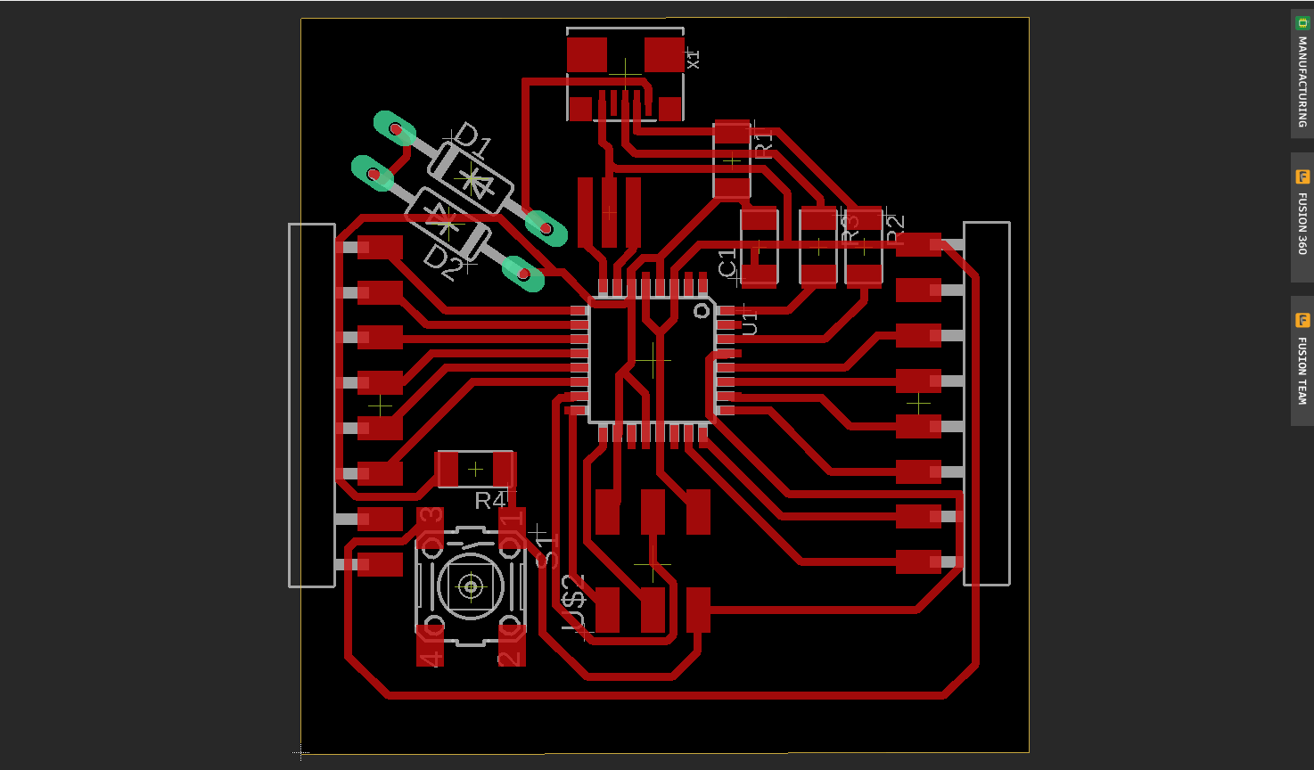
Now that the design was done, it is time to make the PCB, which is when the hell began. I generated the gcode using mods like in Electronics Production assignment, using the same settings.
PCB Manufacturing
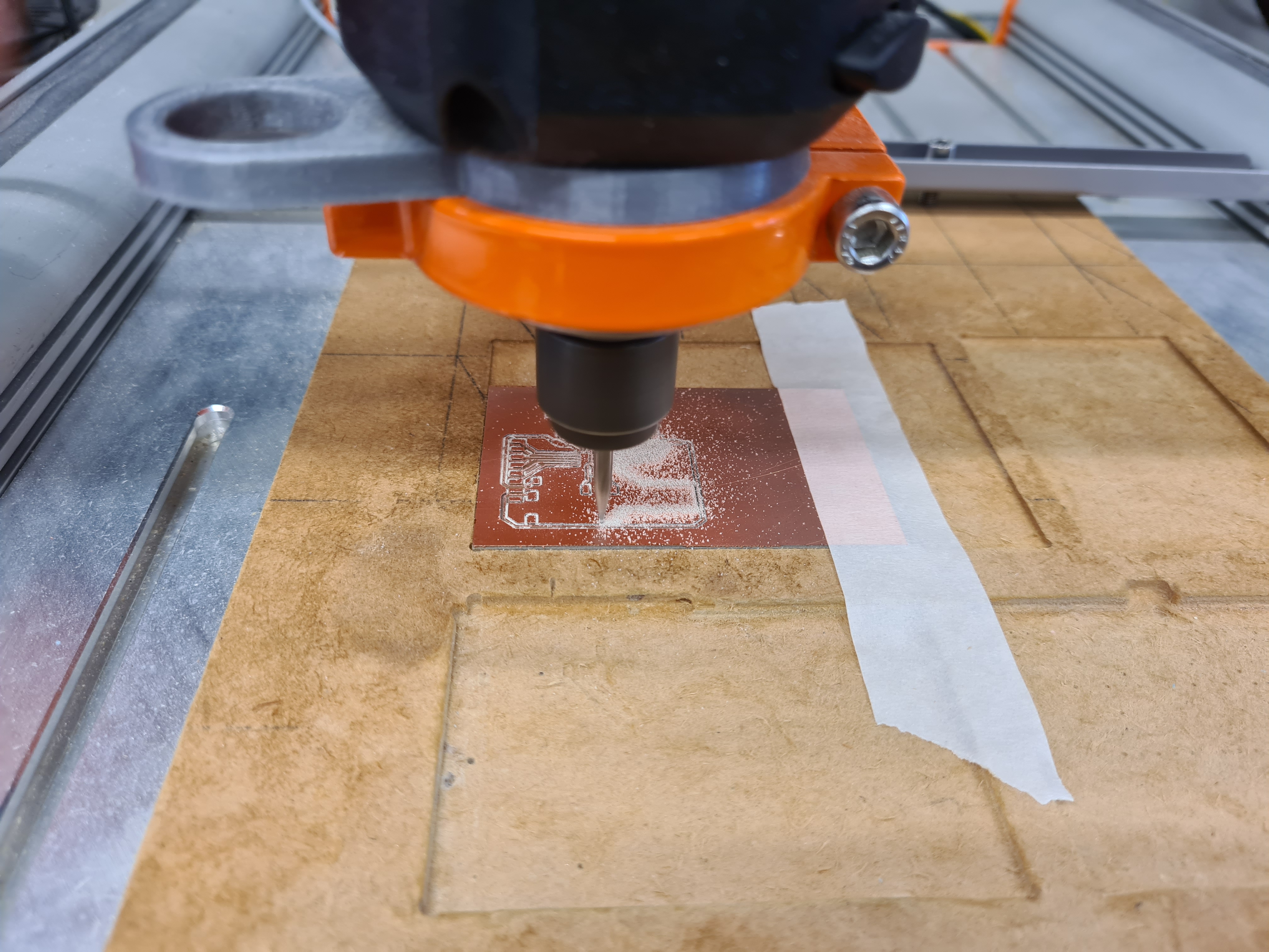
Because I made the PCB fit in the small PCB blanks, I could go in anytime to use the CNC machines. However, I faced a lot of problems with the manufacturing. One was that the number of "good" bits were very little. As it was near the end of the semester, most of the 10 degree bits have chipped or broken off. Still, I found a decent bit and tried to mill it for the first time.
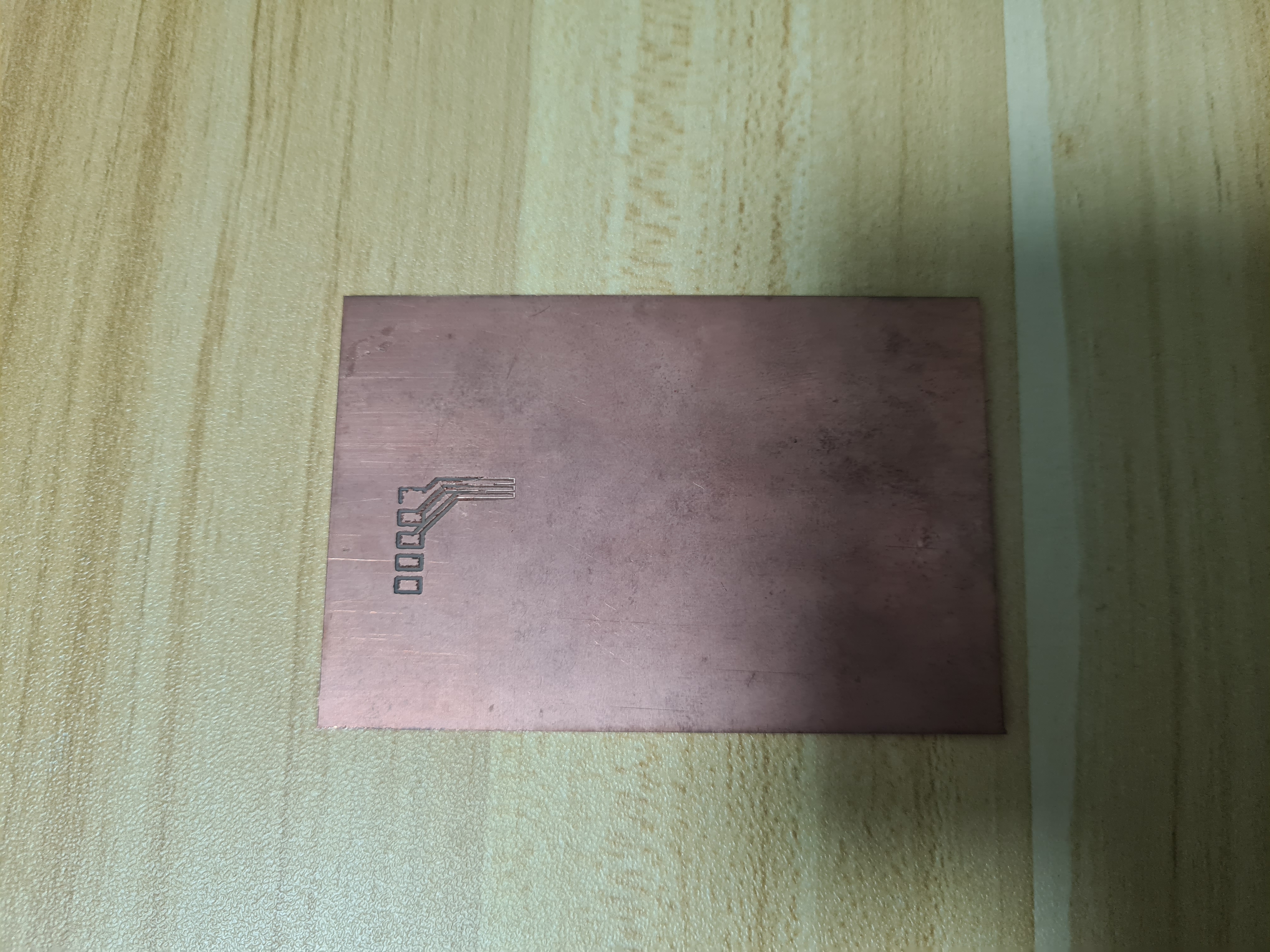
And it was an immediate failure. Even though the first few cuts went well, but then the mill just stopped cutting deep enough. I thought this was just due to me not pressing down the PCB blank hard enough, so I tried again, and again.
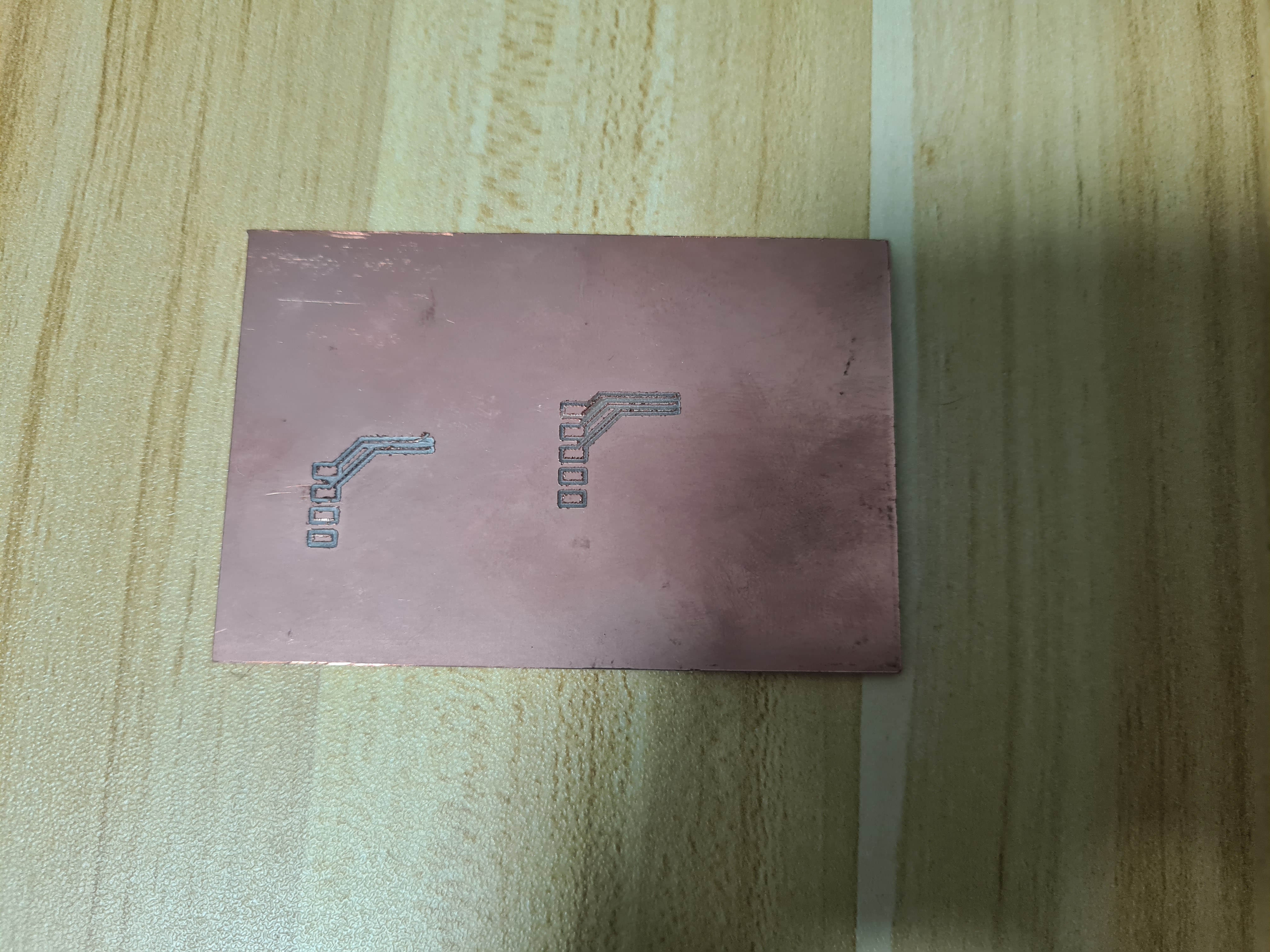
This time, the PCB was cutting too deep. I tried 2 times on the same PCB as a test. Both times, the traces seem too thin and were being ripped. For this test, instead of using the Z-probe for the cnc machine, I used a paper method recommended by my classmate Zi Hon. The first one still seemed too deep, so i upped the height by 0.025, half the depth of cut. Even then in the second test, the trace still seems too deep. At this point, I switched to a different machine and tried another time.
The first trace (the pad on the bottom right) went really well, so I thought that it was at the correct depth. Then it did the third pad and trace and it all went downhill. Still, I just let it continue to see how it goes. This was when it got weird. Even though the depth of cut never changed, the middle of the PCB cut perfectly fine, but the rest was still unusuable.
This attempt was my best PCB of the day, and even then half of it is unusable. I thought that it was no longer a depth of cut problem and more that the PCB was uneven, which was weird because I hammered it down. At this point, Zi Hon wanted to try helping me mill the PCB.
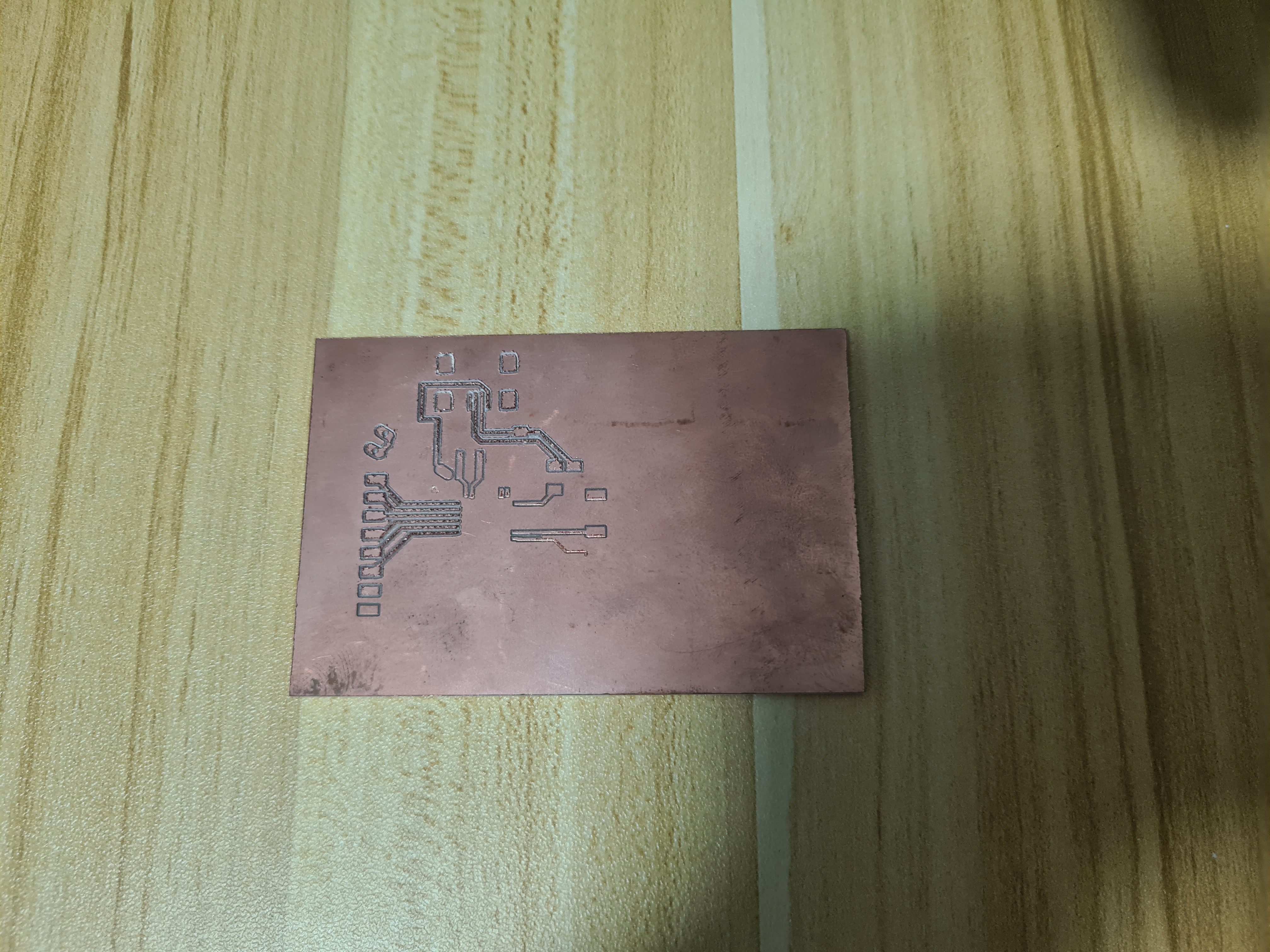
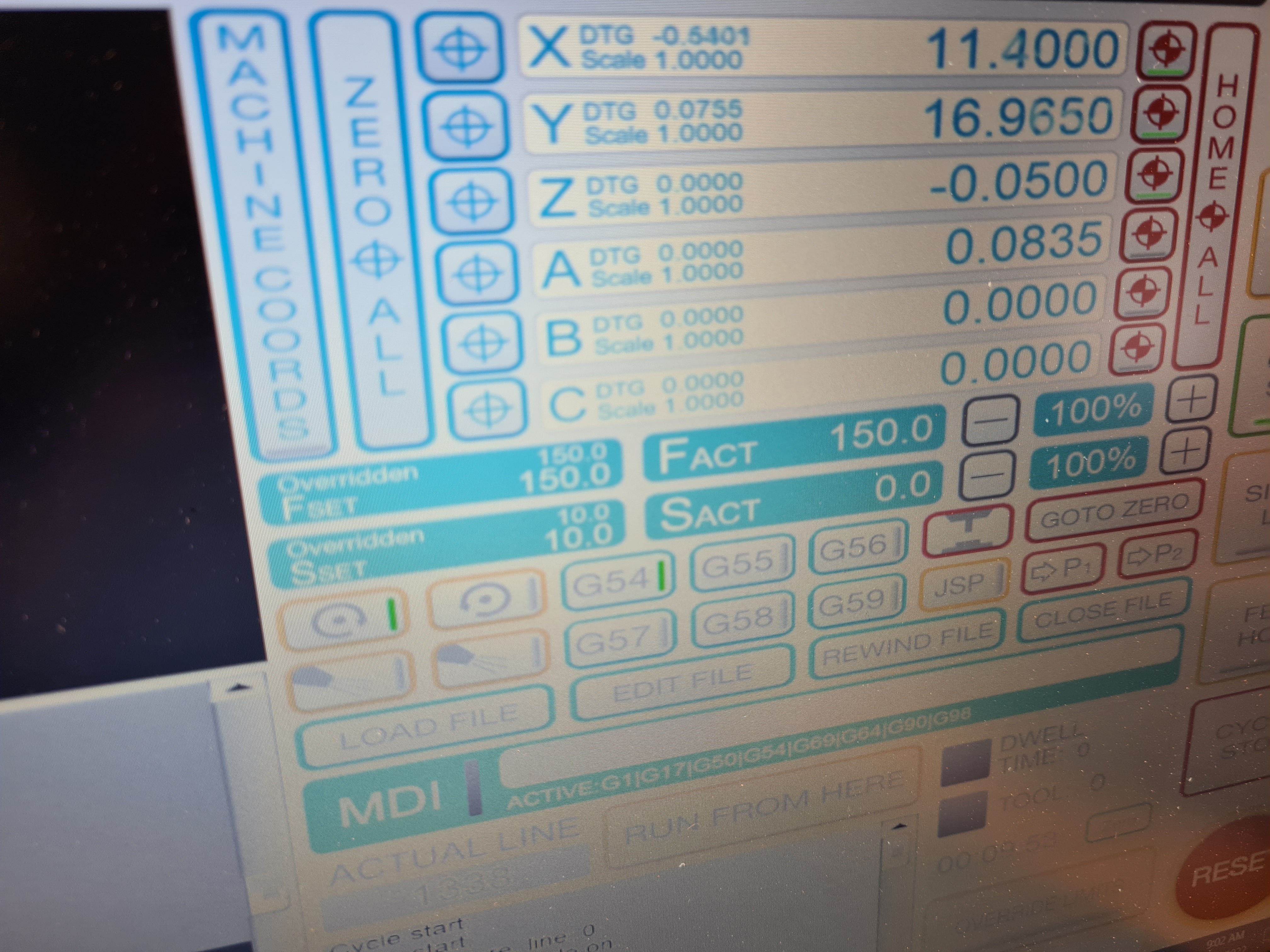
Even though he got his own PCB's milled well, he had no luck with mine. Even on the same machine, it ended up somehow worse than the previous attempt. At this point I wanted to give up and went to Mr Steven Chew, who asked me to send him the Eagle Files. After a few days, he helped me set up the PCB again with a modified board setup. He said he spaced out the componenets to make it easier for me to solder. This time he set it up in a different pocket of the same machine I used previously, with a different bit, a different feed rate of 150 and 2 passes instead of 1.
At first, I thought that it was also cutting too deep because there was more dust than what I was used to, but Mr Steven Chew said that it was a normal amount of material, so I just accepted that and let it run.
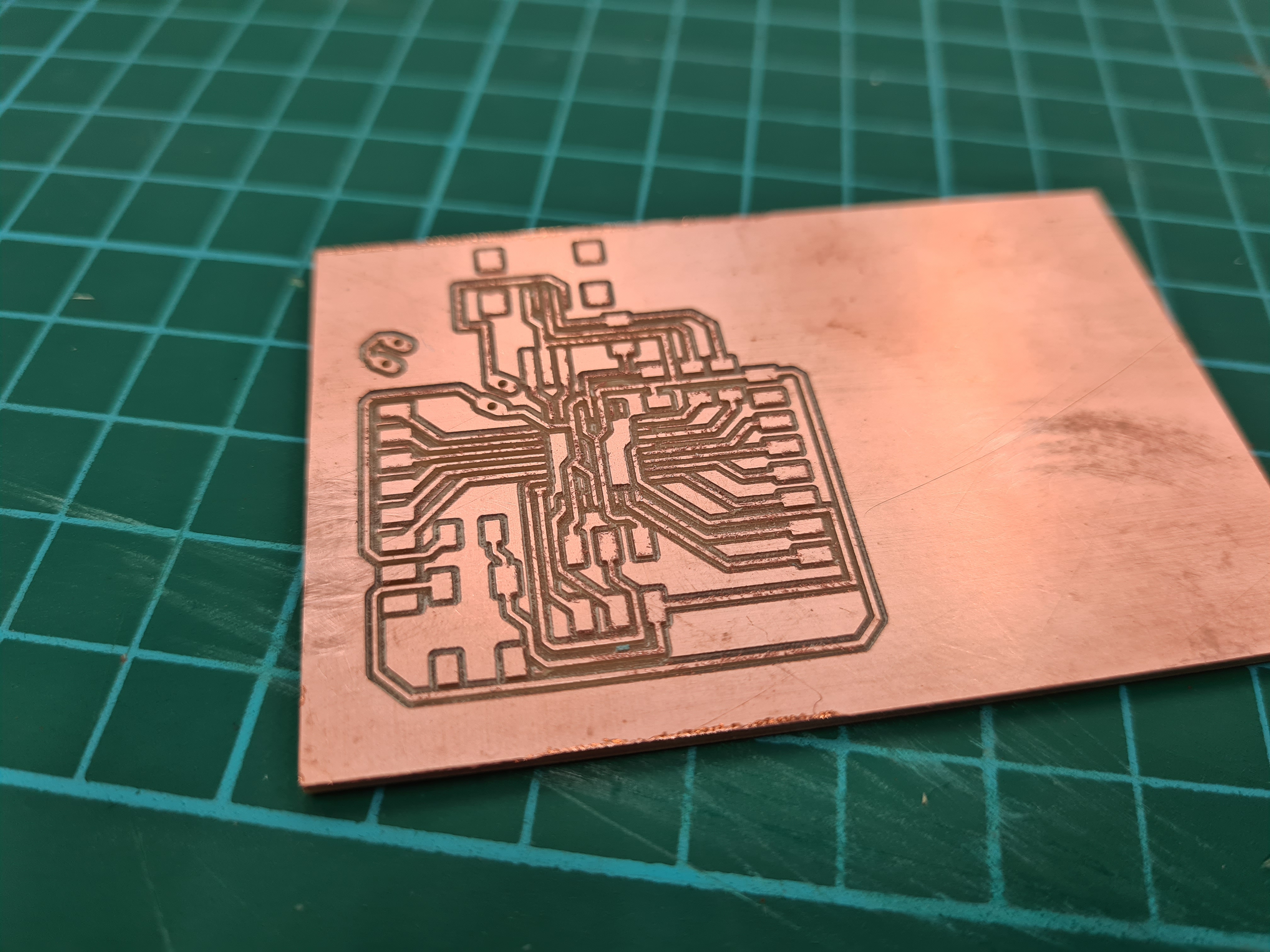
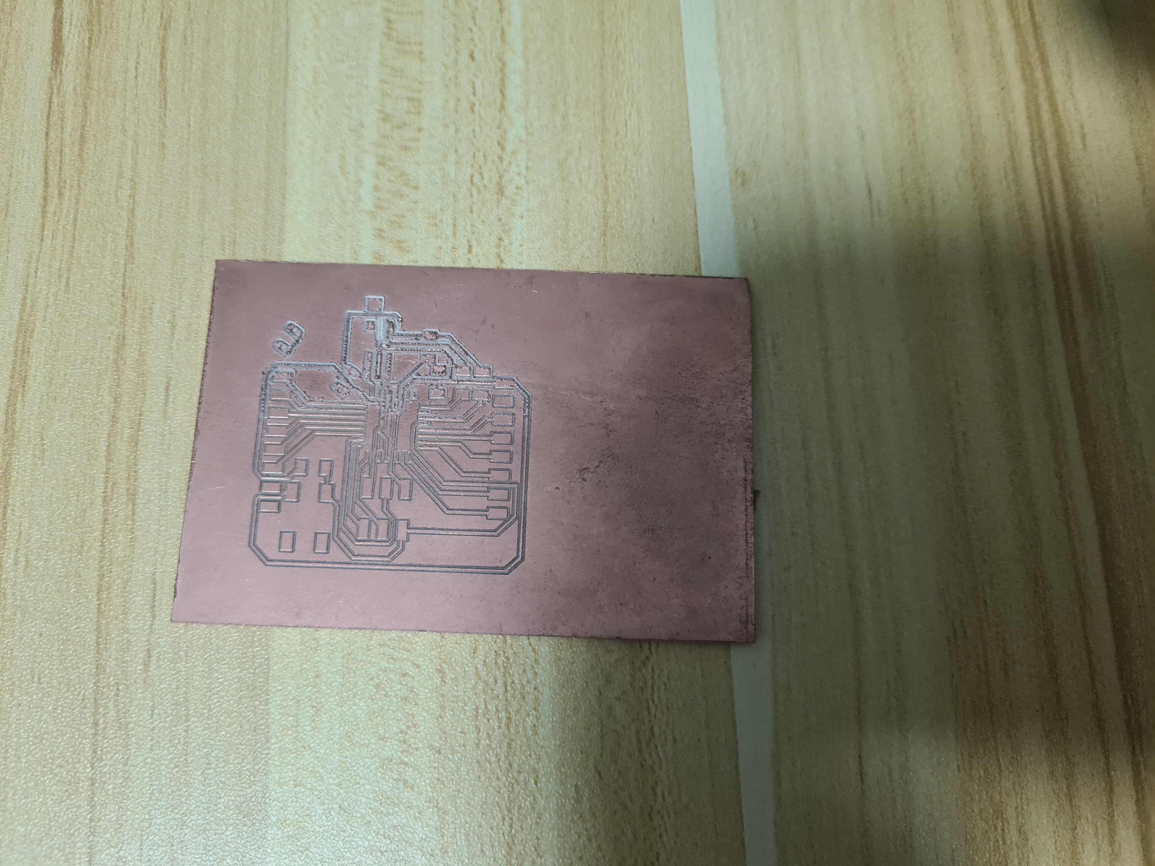
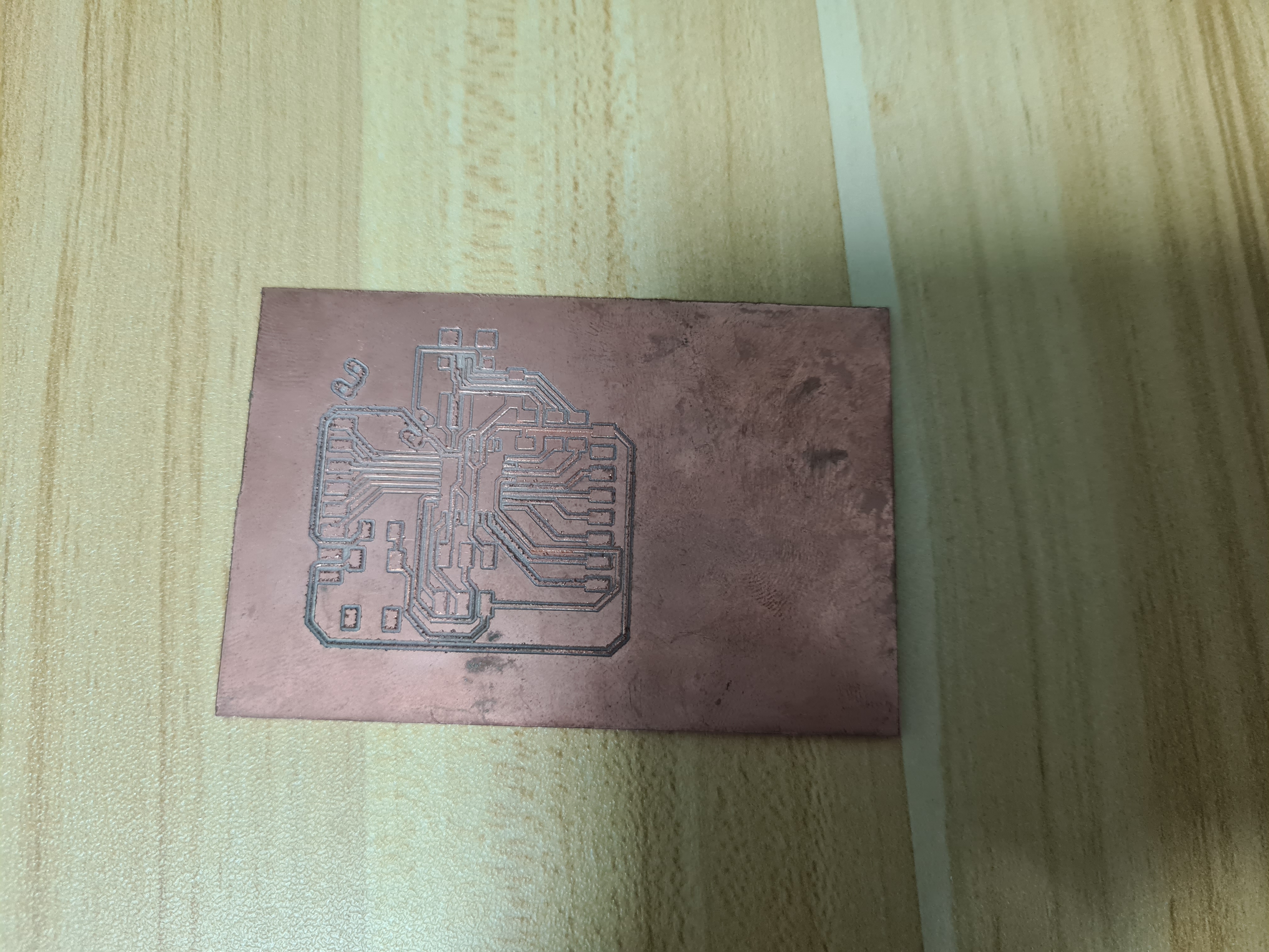
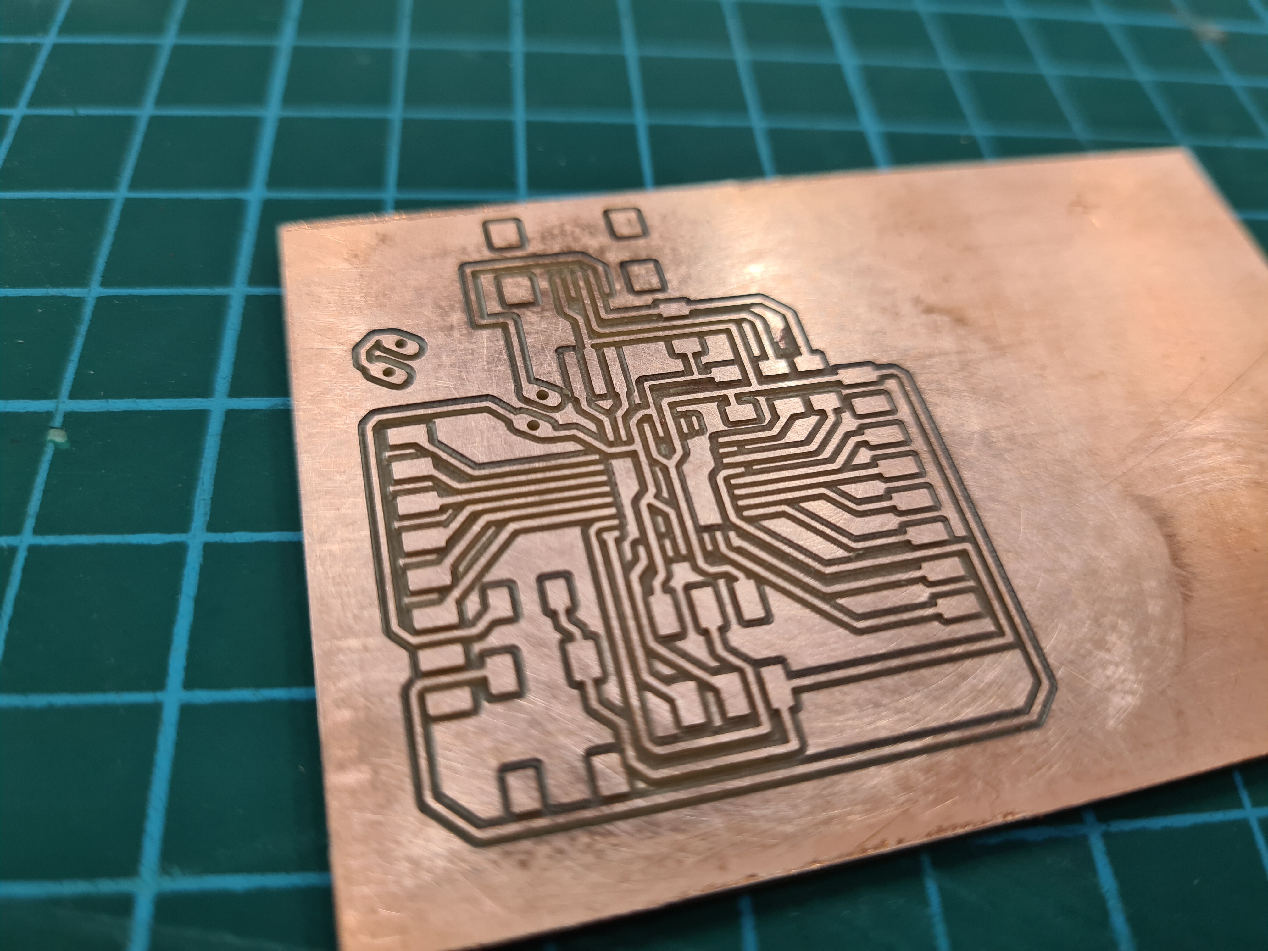
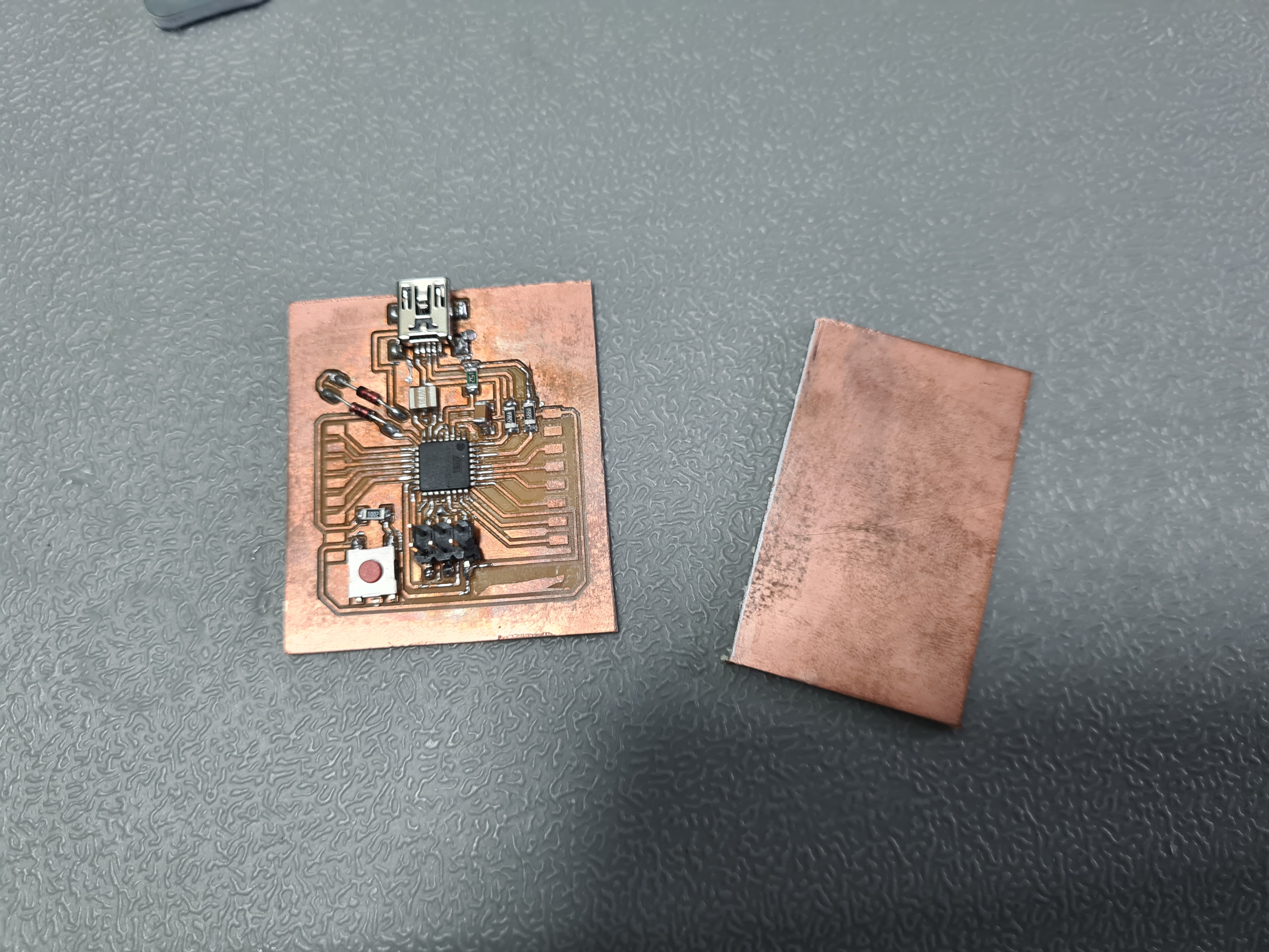
Finally, I got a good PCB mill done. The traces came out perfect, even the small mini usb traces were well milled. I think that my previous failures were due to a blunt bit, where even if the tip was sharp and the depth was correct, the bit was tearing up the trace, causing it to be thinner than normal. At this point, I just took what I got and moved on. Honestly, I am kind of glad I went with the smaller design, because I cannot imagine how much worse a large PCB would be.
I gave it a quick pass with sandpaper to knock down the little burr left on the traces, and went on to solder.
Stuffing the PCB
The components I needed to stuff the PCB are:
- Atmega328 x 1
- 49 ohm resistor x2 (replacing the 68 ohm resistors in the schematic)
- 10k ohm resistor x 1
- 15k ohm resistor x 1
- Female mini usb x 1
- 1N4148 Diodes x 2
- 16 MHz resonator x1
- 6mm switch x 1
- 10uF capacitor x 1
- 0.1uF capacitor x 1
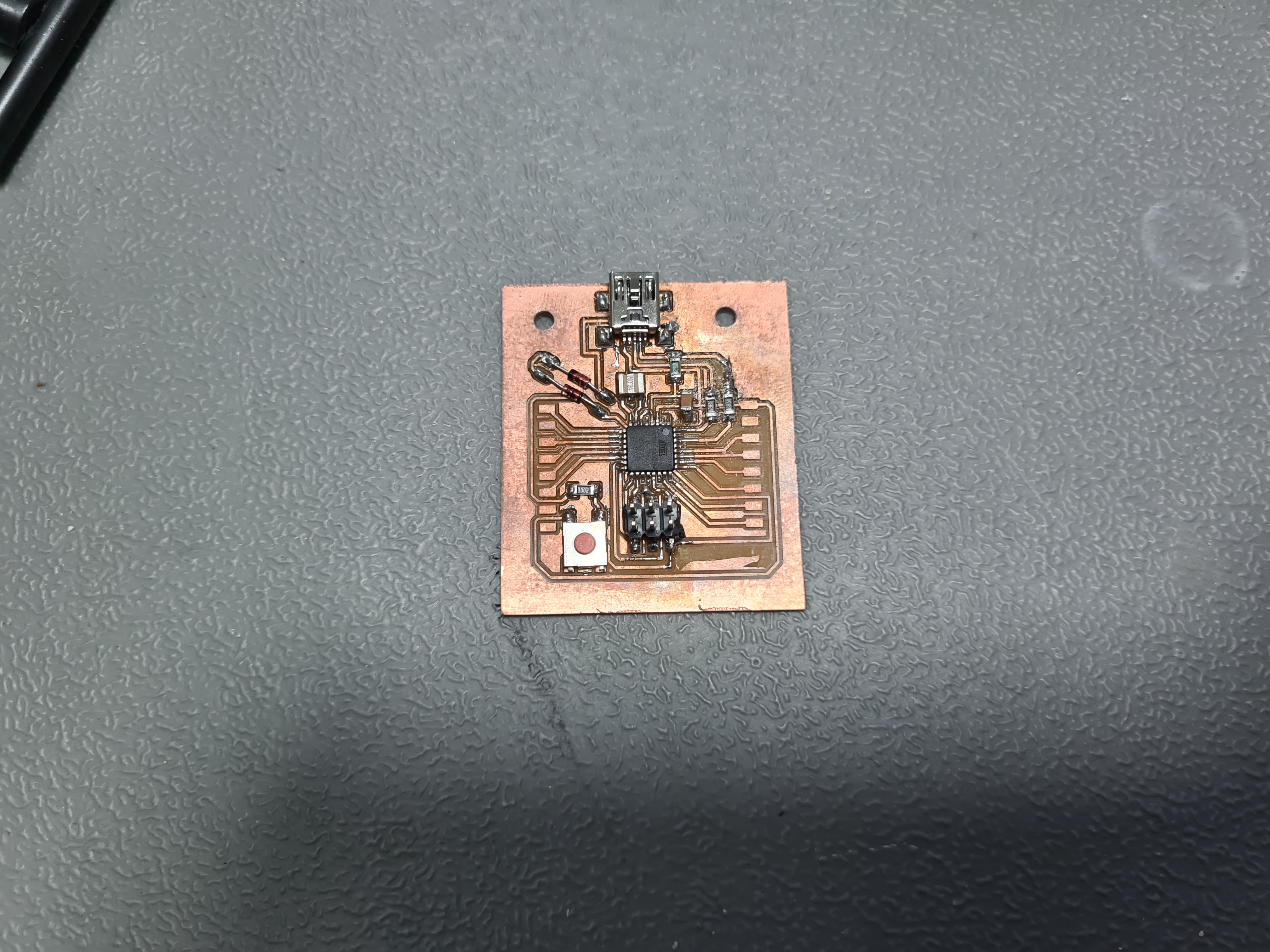
Referencing the schematic and board earlier, I started with the hardest part, the atmega328. Similar to how I did the attiny, I first started at one of the corner pins.
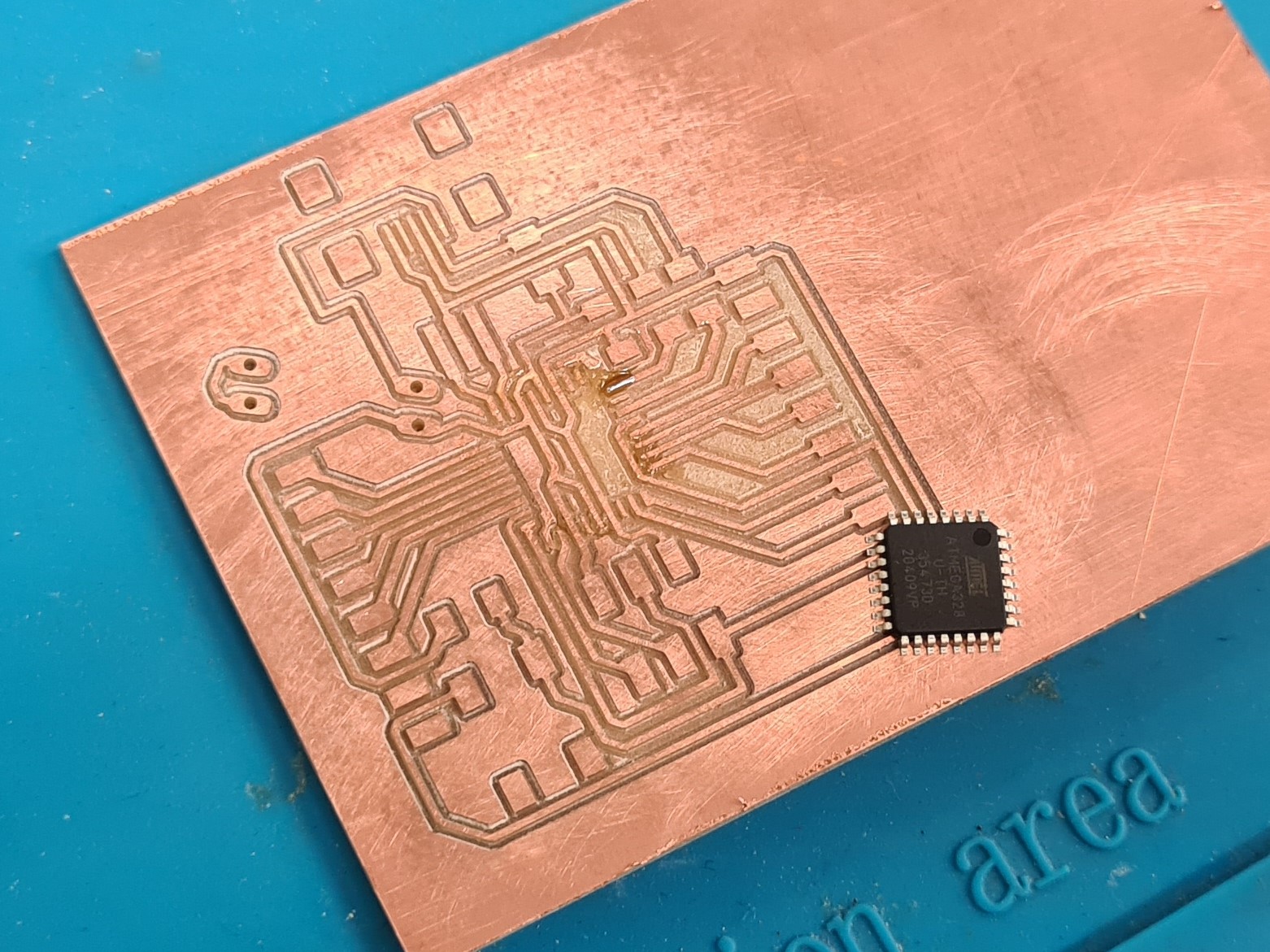
Although I soldered my programmer and hello boards before, the pins of the atmega328 were tinier than I imagined. Zi Hon helped me a lot here, and taught me how to solder the pins efficiently. He showed me on one side of the atmega. He put a lot of flux on the pads of the PCB and the atmega chip. Afterwards, he got a small amount of solder onto the iron and in one pass, dragged the iron over the pins and let surface tension take over. The result is that all the pins were soldered and due to the small amount of solder, there was not enough to short 2 adjacent pins together. I used this method to solder on the rest of the atmega.
After this, I tackled the resonator. As the pads of the resonator completely cover the traces, I had to use the heatgun to solder on the component. I first put a small amount of solder onto the pads, then placed the resonator on it. Using the heatgun, I carefully heated up the pads underneath, taking care to not reheat the atmega. After a few minutes of struggling, I got the resonator soldered on.
At this point, I also tackled the mini usb. After the atmega, this was not really that bad, and it went down well.
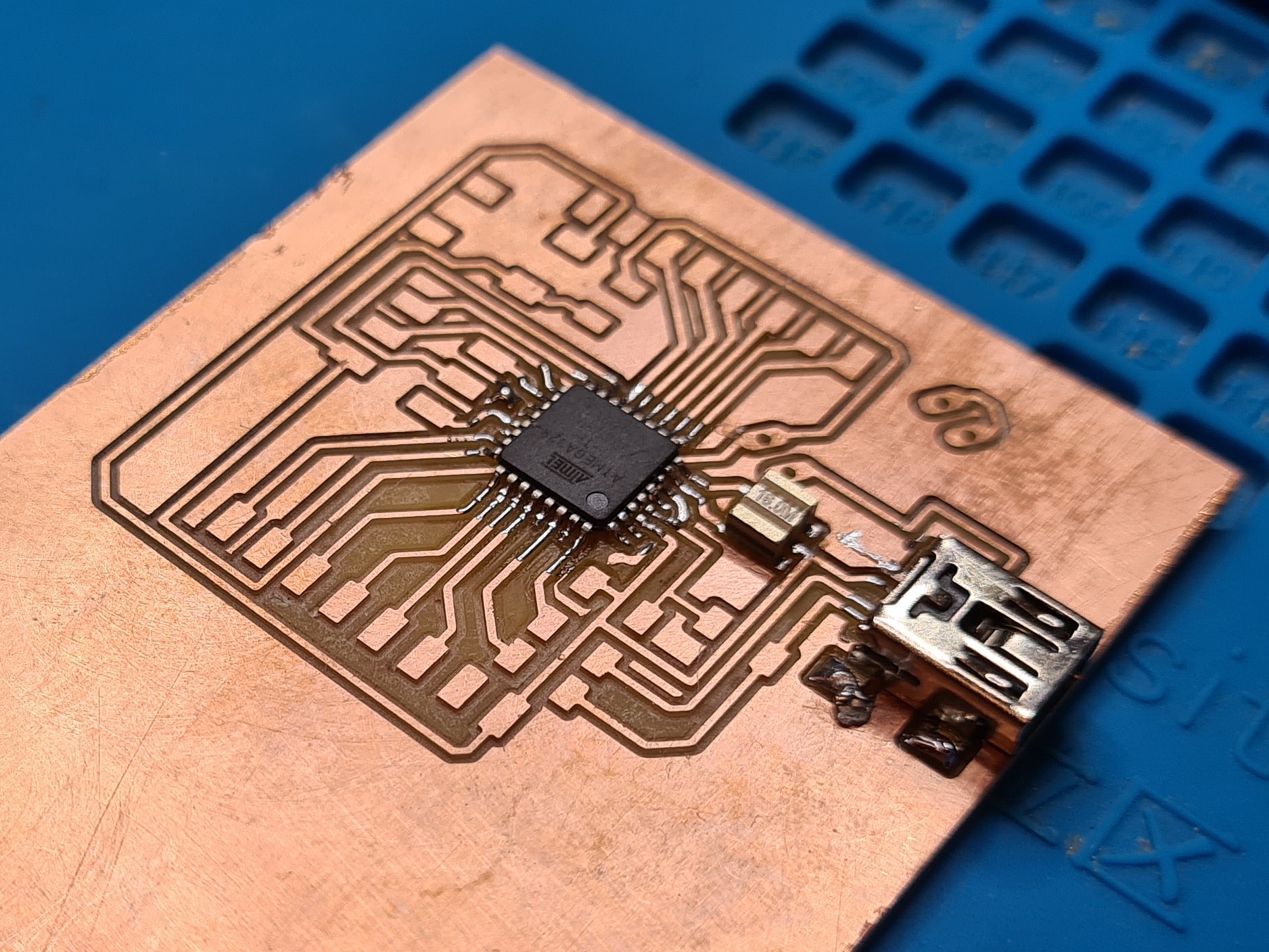
This was when I encountered an issue, not a major issue but just something to take note of in the future. When soldering on the housing(?) of the mini usb to the PCB, I accidentally put too much solder on one of the pads and the pad connected to the rest of the PCB (as shown above, near the bottom right). I tried to remelt the solder to remove it, but no matter how long I put the iron on the blob, it would not melt. This is when I realised that, essentially, the large sheet of copper connected was acting like a heat sink to the pad, and all the heat I was adding to the pad was being removed just as quickly and being dispersed. After a few minutes, I just gave up and left it as is, as it did not affect other components anyways.
The rest of the components went down well. The only issue I faced was that I forgot that 2 bypass capacitors were needed, but I forgot it in the design. Luckily, the capacitors are supposed to be in parallel, so I just stacked the 2. Unelegant, yes, but I had no other options really. And with that, the PCB is (mostly) done and I tested it using the programmer.
Testing the PCB
I opened up terminal and ran "avrdude -pm328 -cusbtiny", and it was able to recognise the chip, which is good news. That means that I can try programming this using arduino IDE to test.
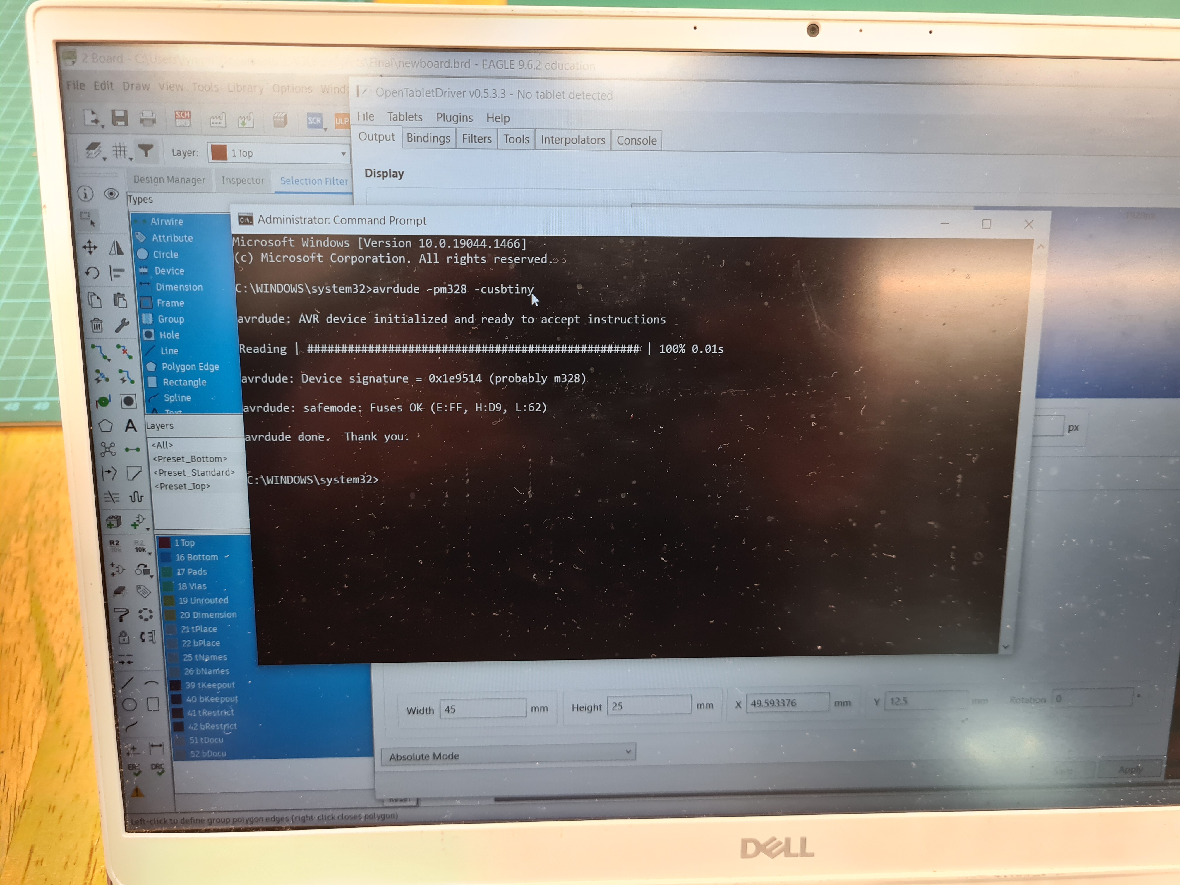
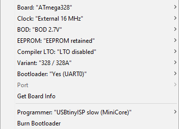
To setup arduino IDE to program the board, I used the Atmega328 core by Minicore. Installing the core is just like in my embedded programming assignment. Copy paste in "https://mcudude.github.io/MiniCore/package_MCUdude_MiniCore_index.json" into preferences, go to boards manager and install the core.
Once it was installed, I set up my IDE like so.
I modified the basic blink program in arduino to the different pins that I am using for the keyboard. From the schematic, pins 5-10 and 14-19 will be used for the switches. I just changed the output pin to the pins listed, one by one and tested with a multimeter to see if theres a pulse coming through.
I did not record it but yes it was working so I moved on to the other parts of the project for now.
Case Design and Manufacturing
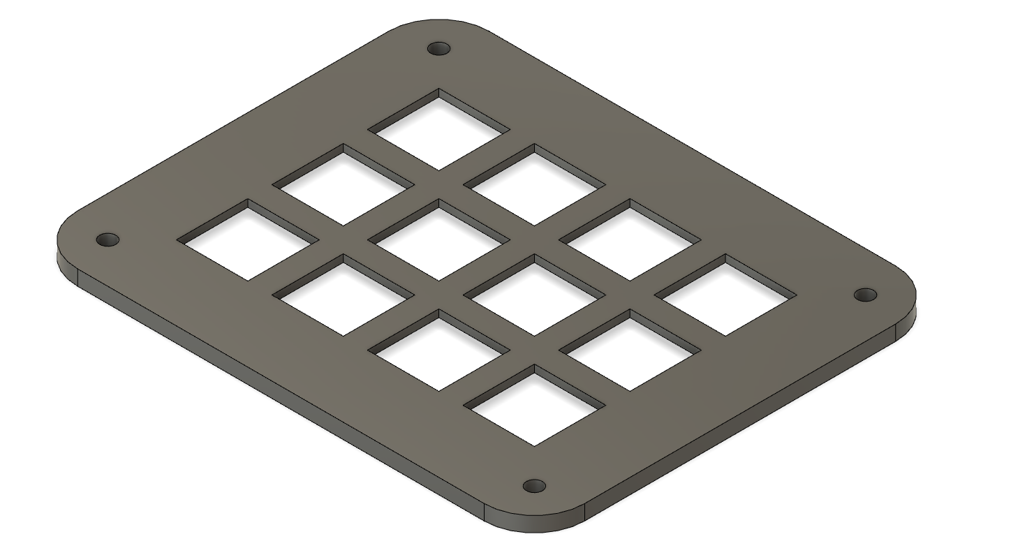
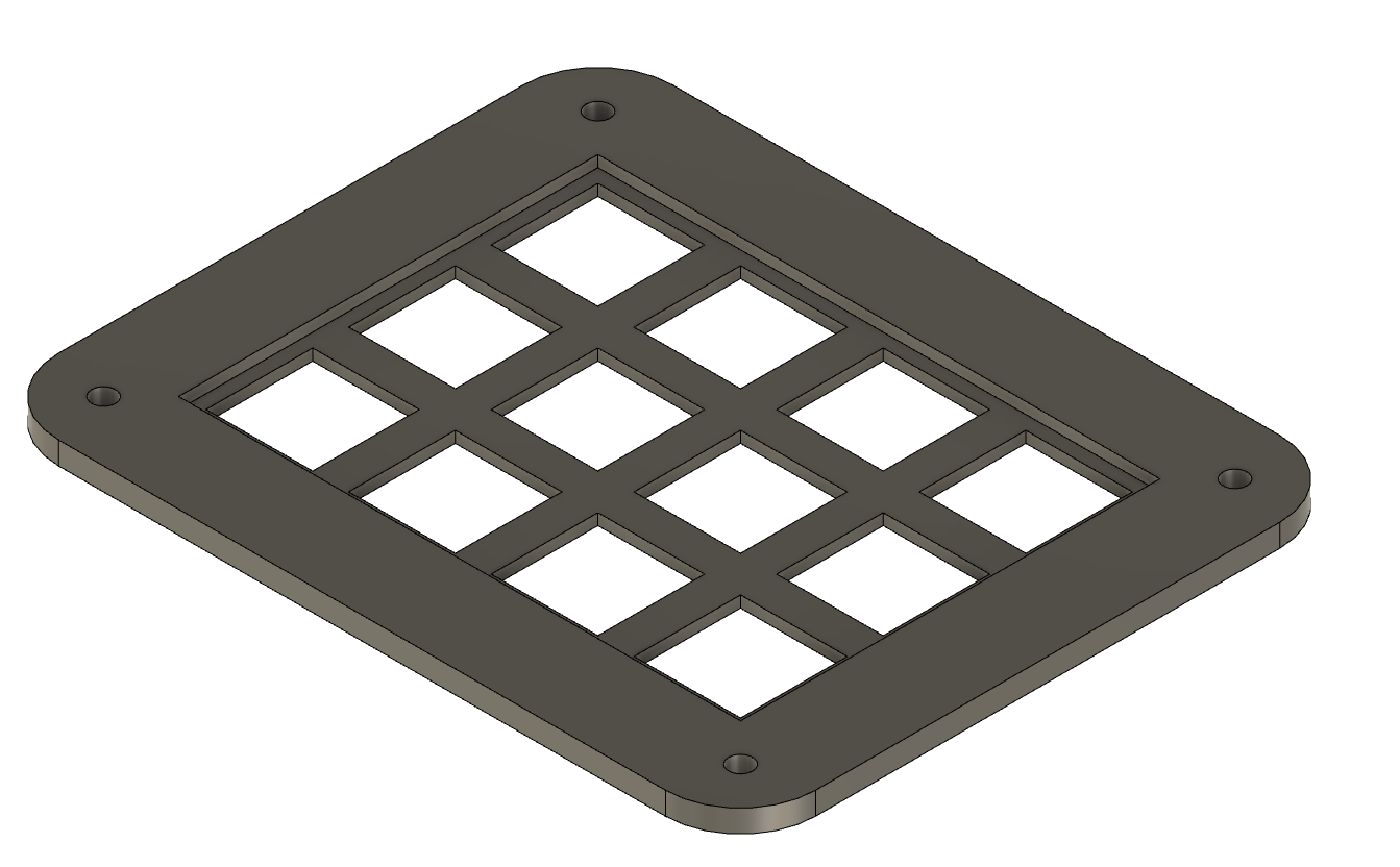
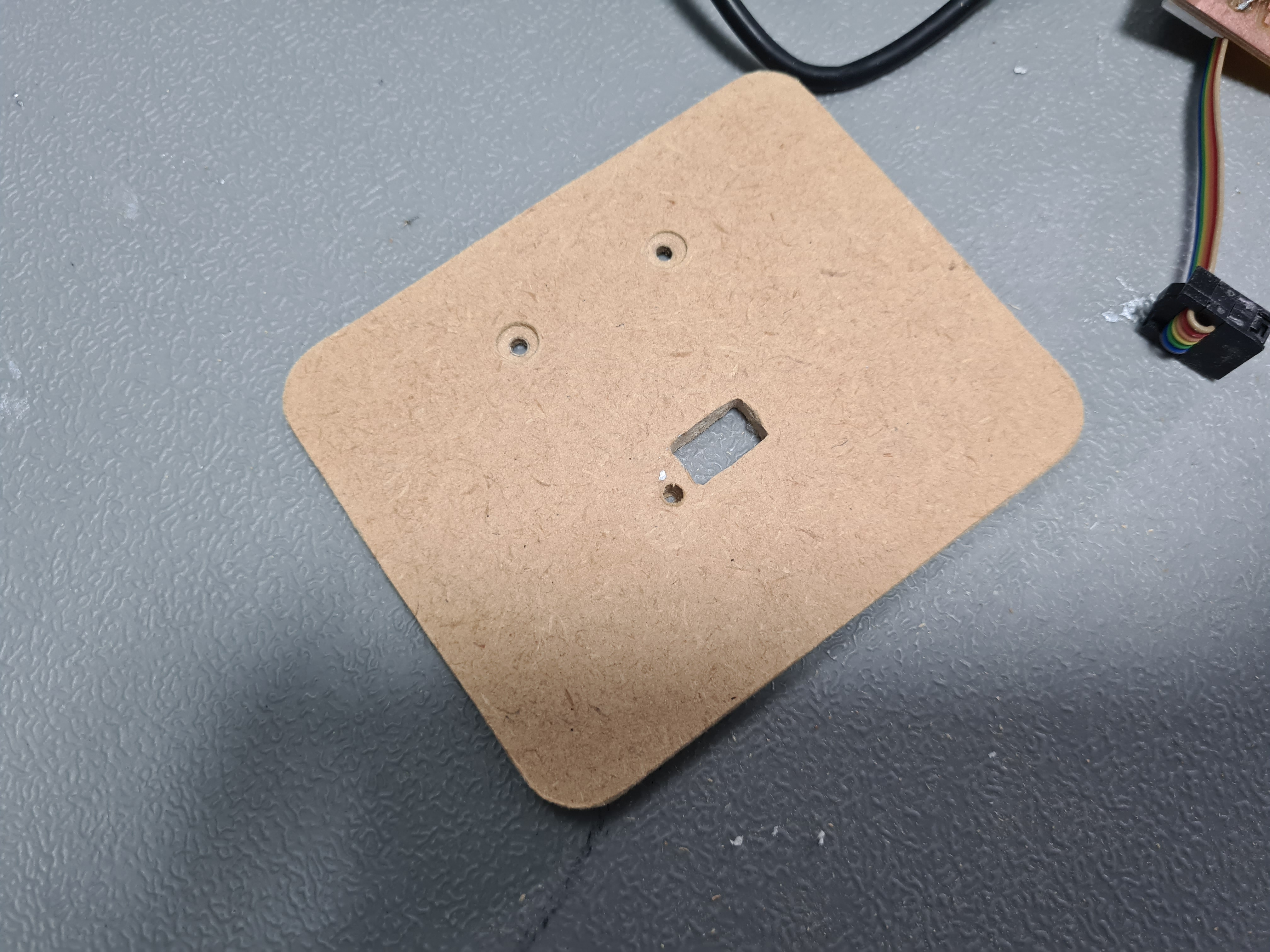
For the case design, I came up with a simple case that I can use the large format CNC and lasercutting for. I first came up with the top plate that will hold the keyboard switches. After taking some measurements of my own keyboard, I came up with this.
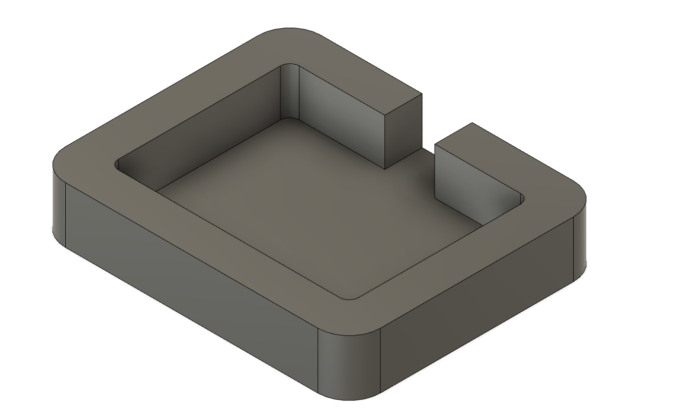
Using this, as a reference, I modelled the bottom case as well.
I first went to laser cut the top plate using 3mm acrylic as that was the part with important dimensions. The plate came out well and the switches were able to fit snugly.
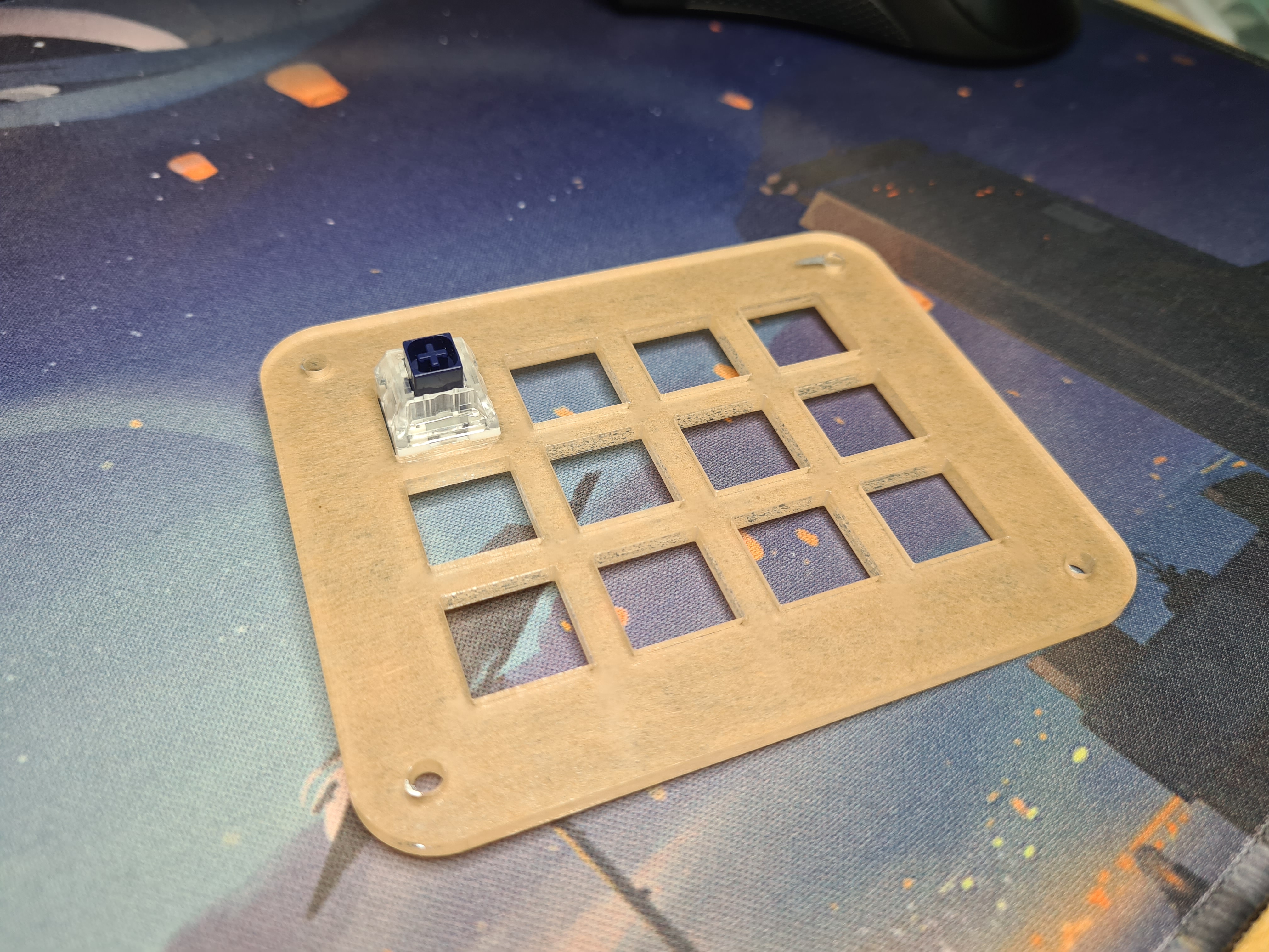
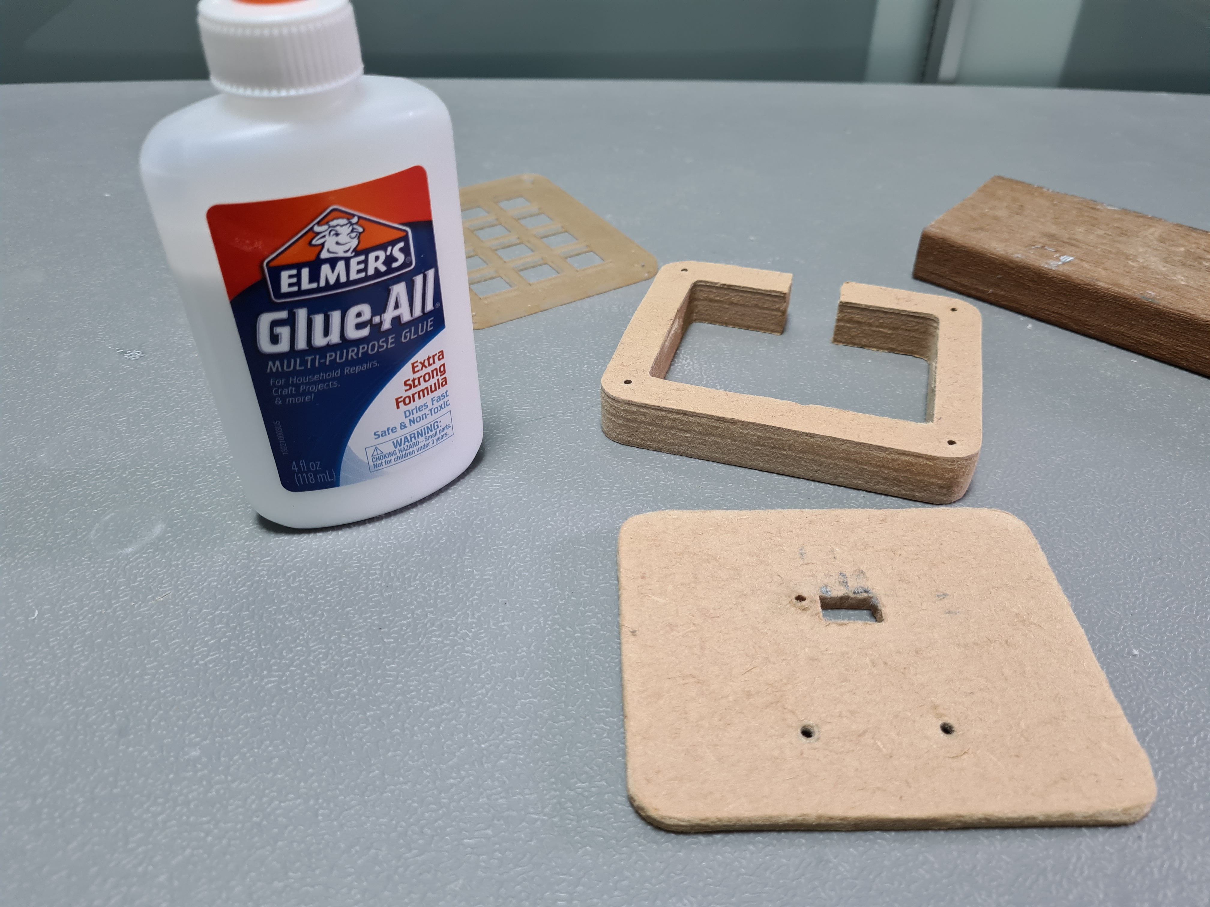
It was now then I realised laser cutting is not ideal. Looking at conventional keyboard plates, the switch has tabs that click into place. However, because of the thickness, the switch was just friction fit into the acrylic, and I could very easily knock it out.
To remedy this, I remodelled the top plate to be thinner where the switches are placed, from 3mm to 1.5mm, as well as taking into accound tolerances of my 3d printer and expanded the squares to be 14.2mm,
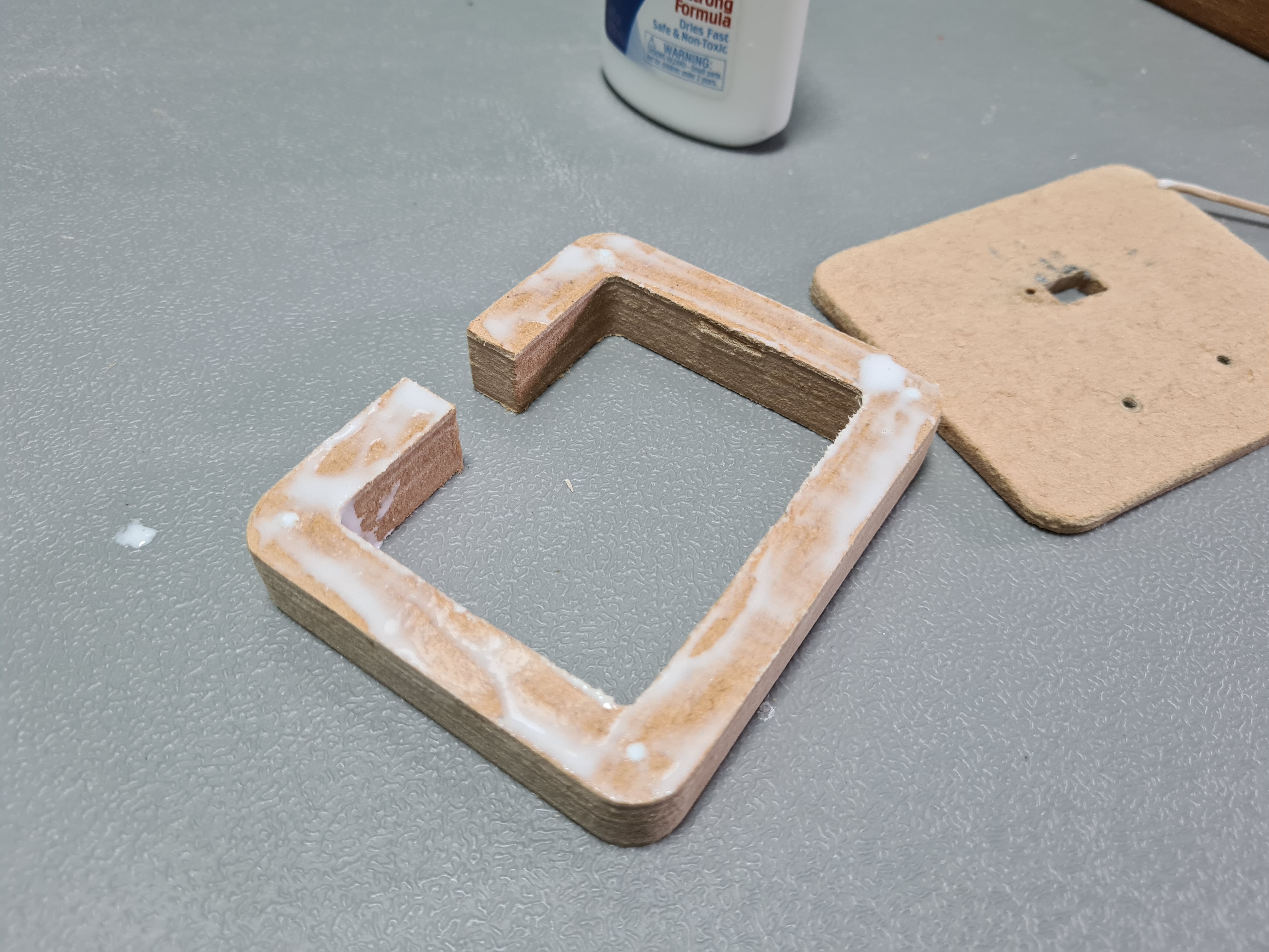
Because of the step in thickness, I just 3d printed the top plate as it was more convenient. In hindsight, I could have lasercut 1.5mm acrylic, but at the time I had no time to go buy a sheet.
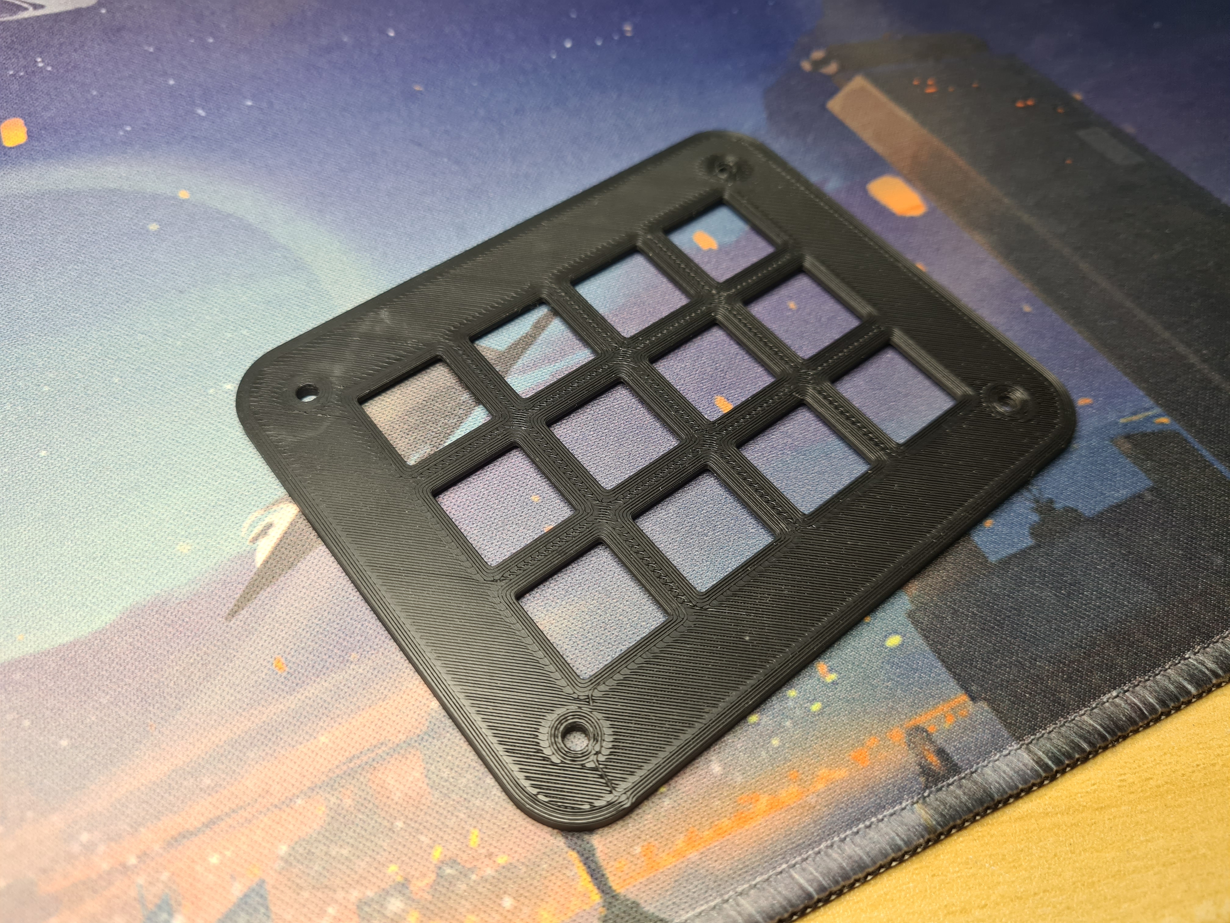
The new plate came out well and I was able to click in the switches firmly. The difference is quite apparant in the picture below.
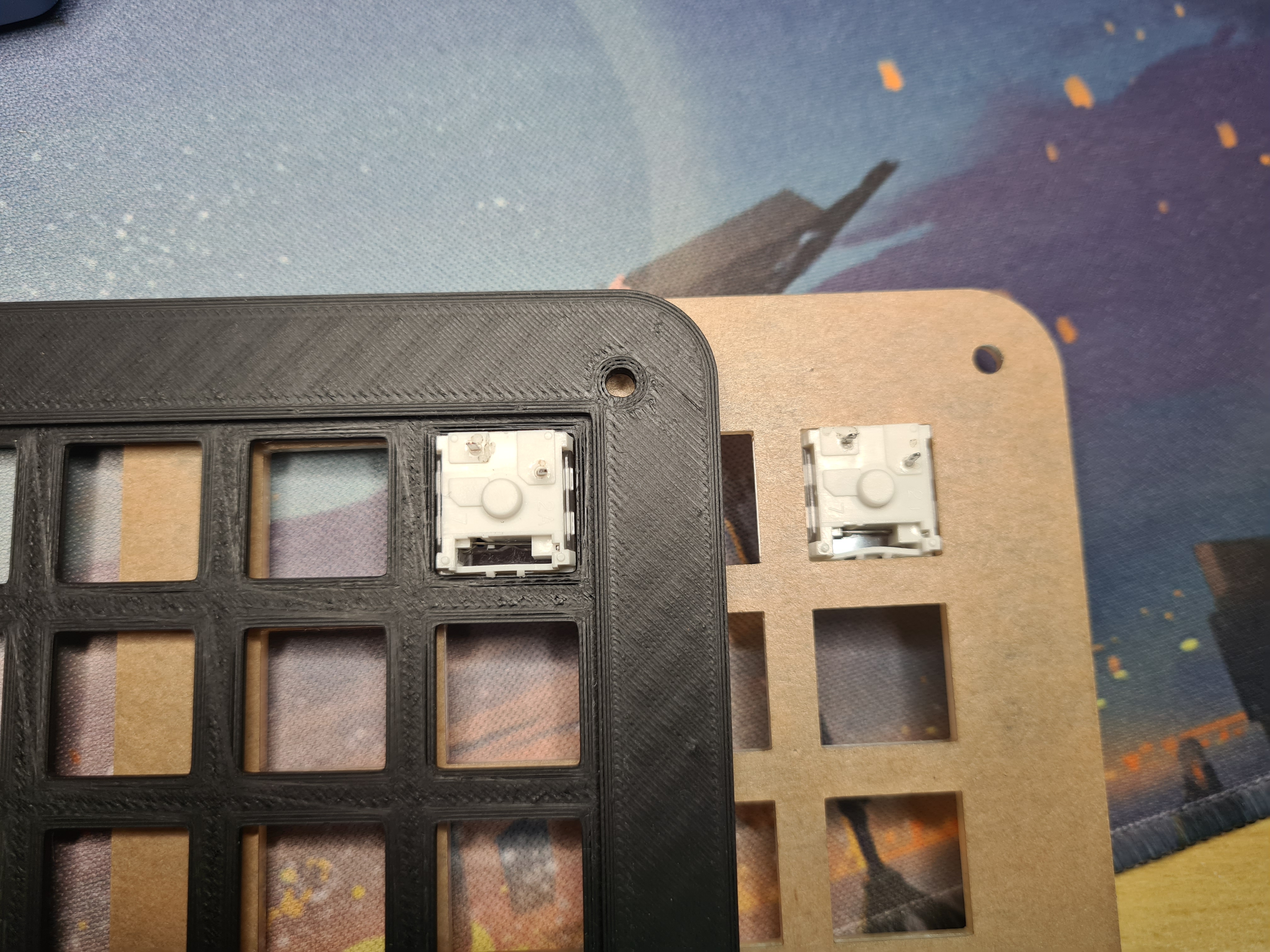
On the left is the proper way of mounting. On the right with the lasercut plate, you can see that the plastic was being bent where the clip is. I decided to move on with the 3d printed plate.
For the bottom case, initially I was planning to pocket and profile a single block of wood. However, when I went down to the large format CNC, they only had 15mm MDF. As I needed 15mm of space internally for my components, I had a dumb idea.
Instead of doing it one piece, I would profile cut the top portion, then pocket the bottom portion completely to 5mm (I was scared of going too thin) then profile cutting it. And that was exactly what I did. I exported the faces as dxf and went down to the large format CNC.
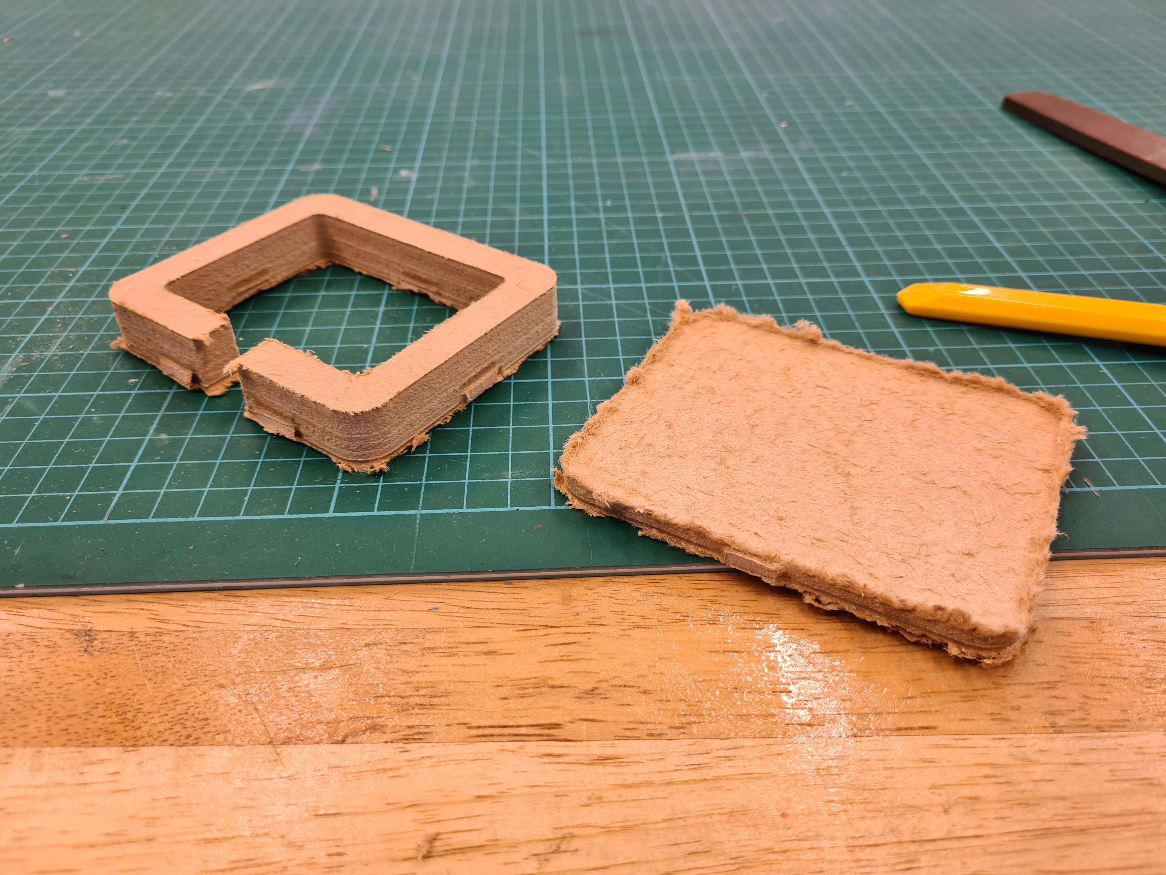
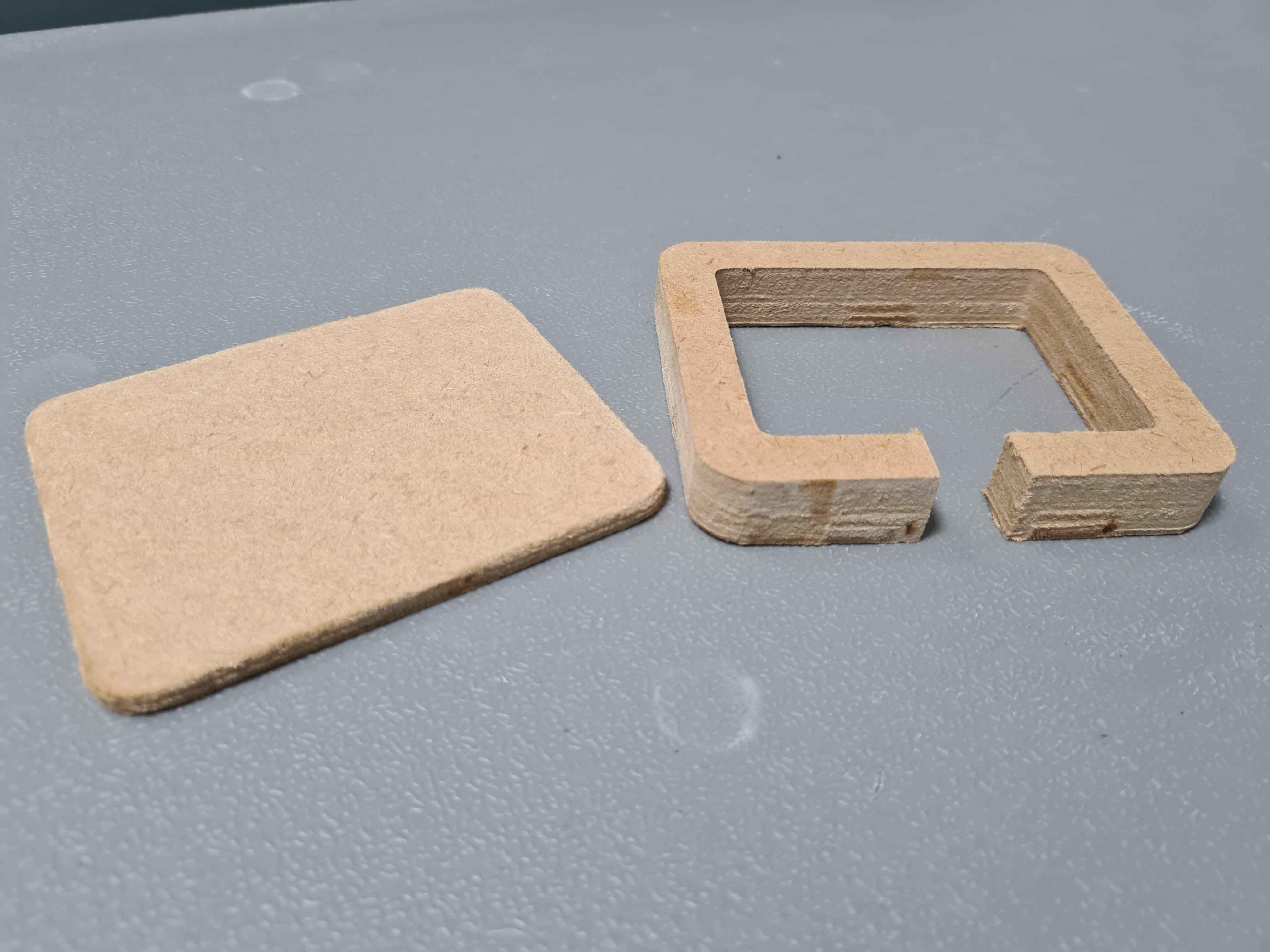
Because of the amount of material being removed, and the material itself, the surface and edges were fuzzy and left a lot of material left over. Using some low grit sandpaper and a knife, I cleaned up the pieces.
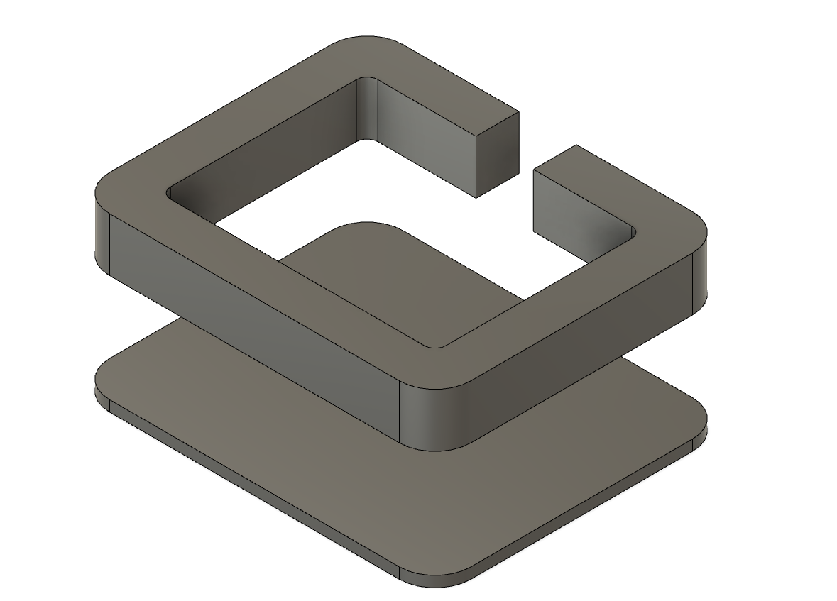
Here is the fusion model of the final case I made.
Now its time to intergrate all the hardware together.
Integration
This is the part where my project strays heavily from digital fabrication and goes into regular fabrication. I could have put more thought into the process but I didn't, so oh well.
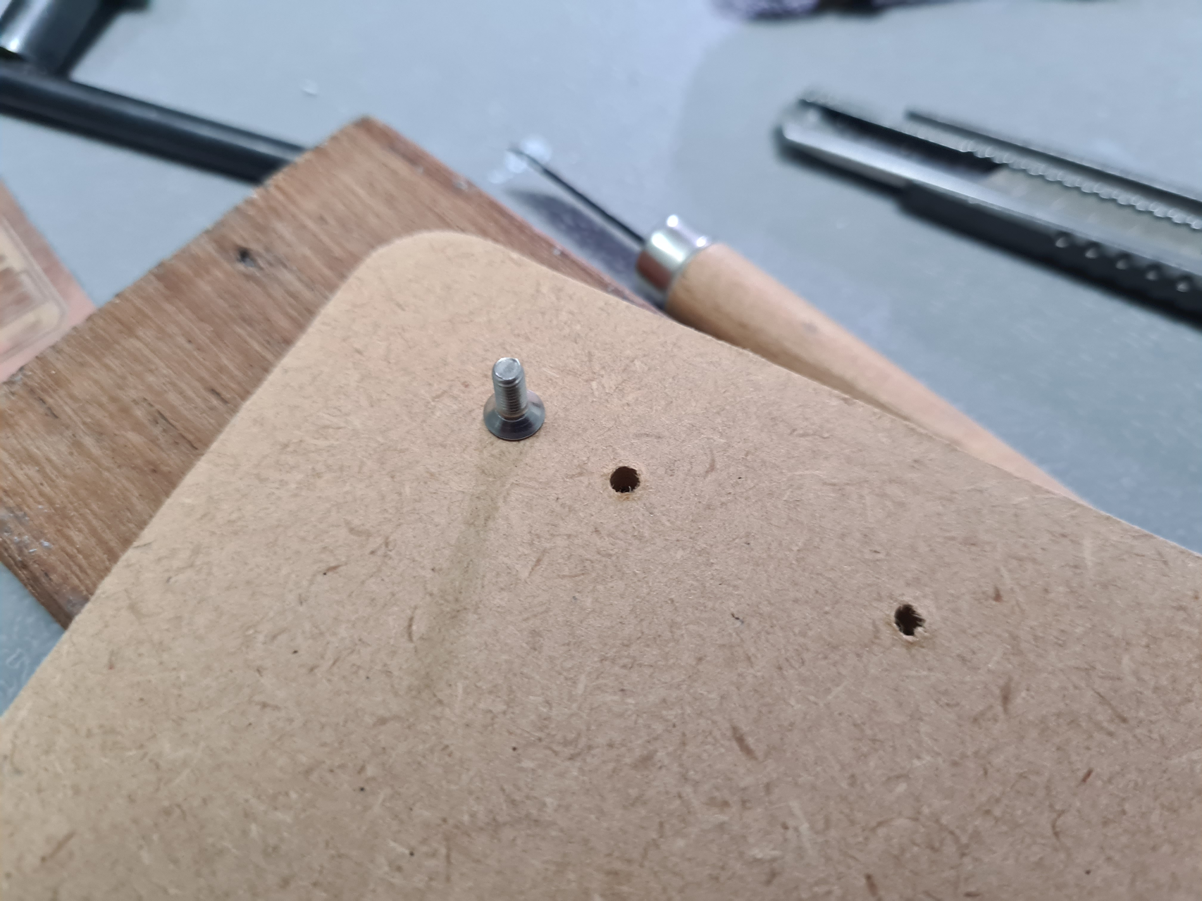
First things first, the PCB is too big. The USB port does not line up with the center opening I made for the case, really just an oversight on my part. To solve this issue, I took a hacksaw to the pcb.
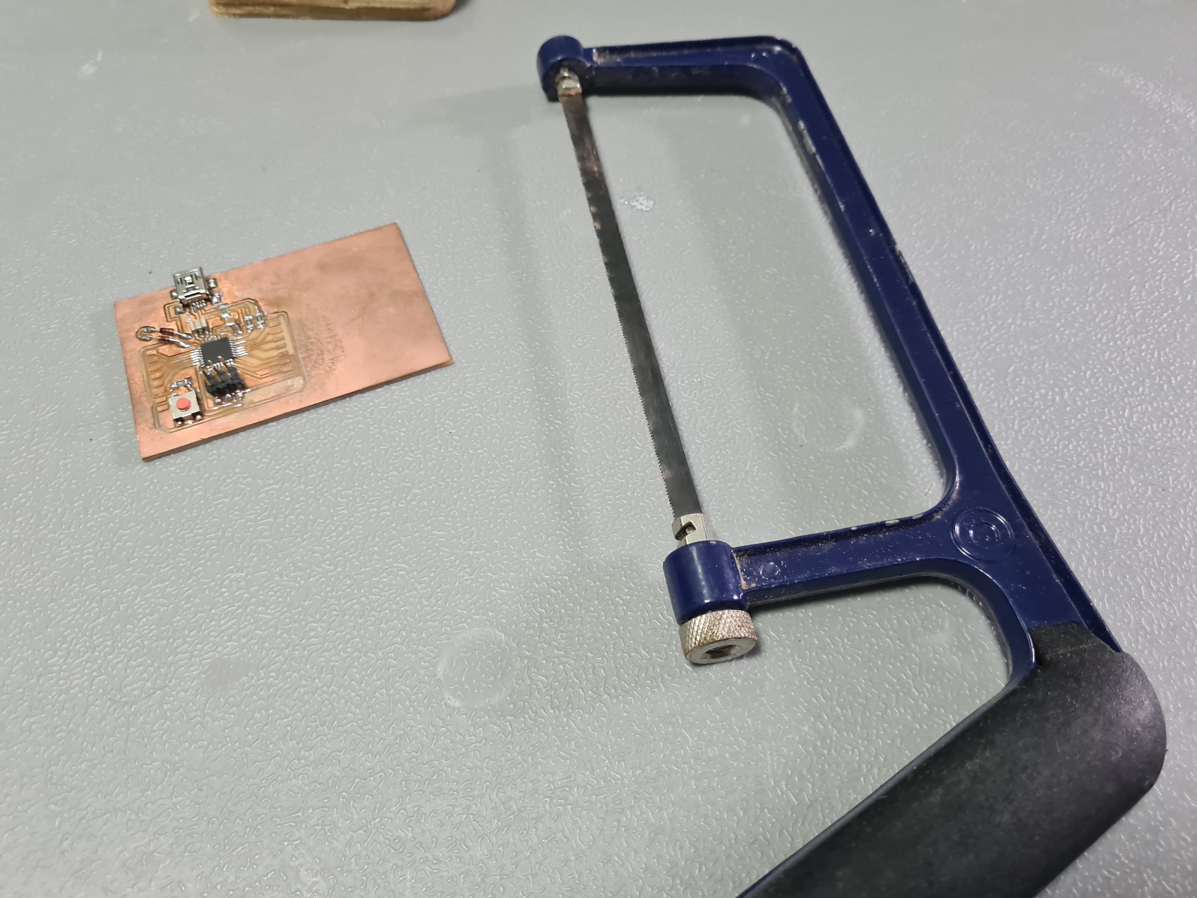
I am surprised I didn't break anything during this. After this I realised I had no way of mounting the PCB properly (double sided tape does not count). So to solve this problem I have created for myself, I took a drill to the pcb.
Using the PCB as a guide and guesstimating the alignment, I drilled similar holes into the bottom plate of the bottom case. I plan to use m3x5 countersunk screws in the build as I wanted it to be flush with the bottom, so after the 3mm holes were made I used a 6mm bit to somewhat countersink the screws.
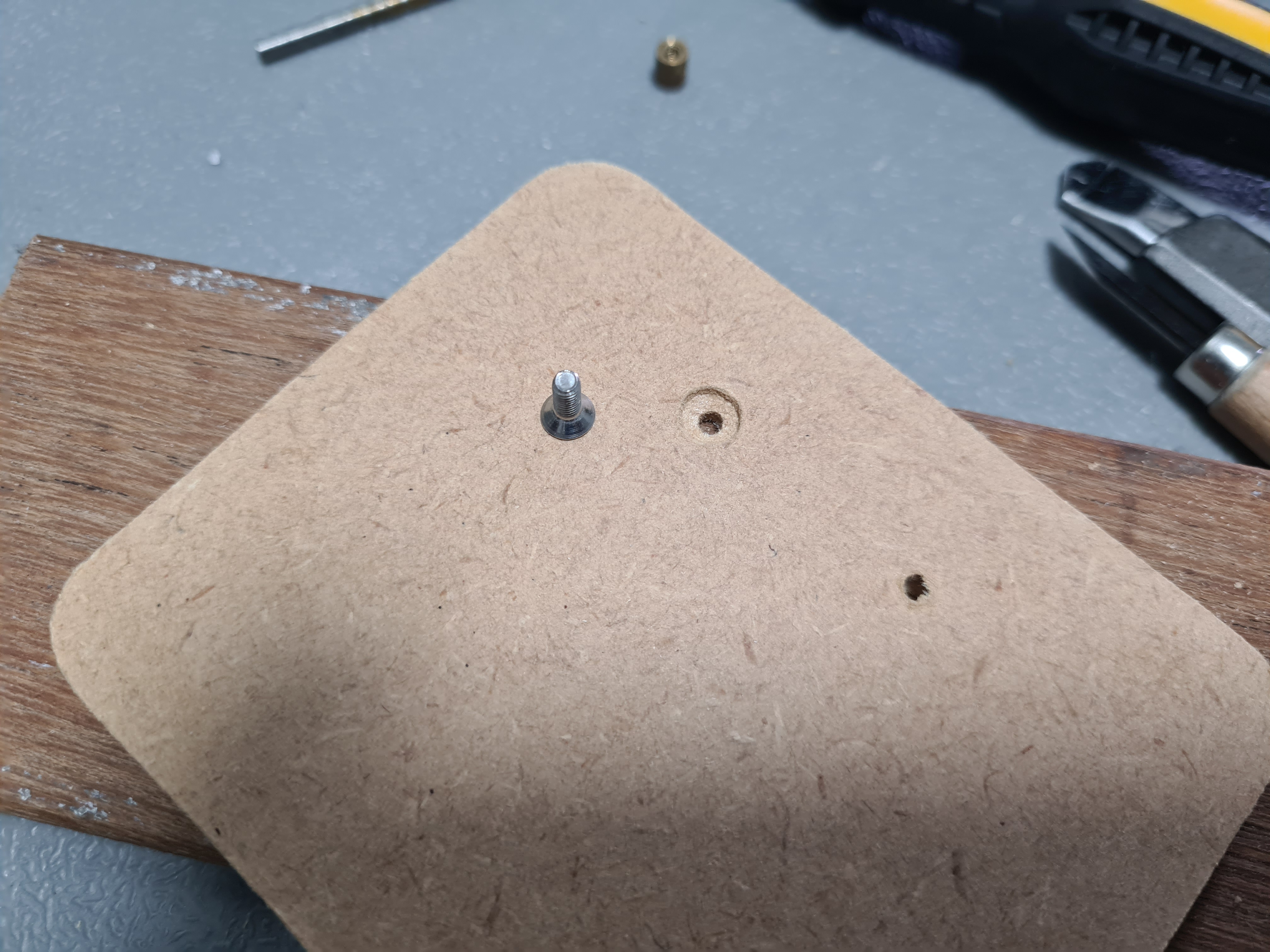
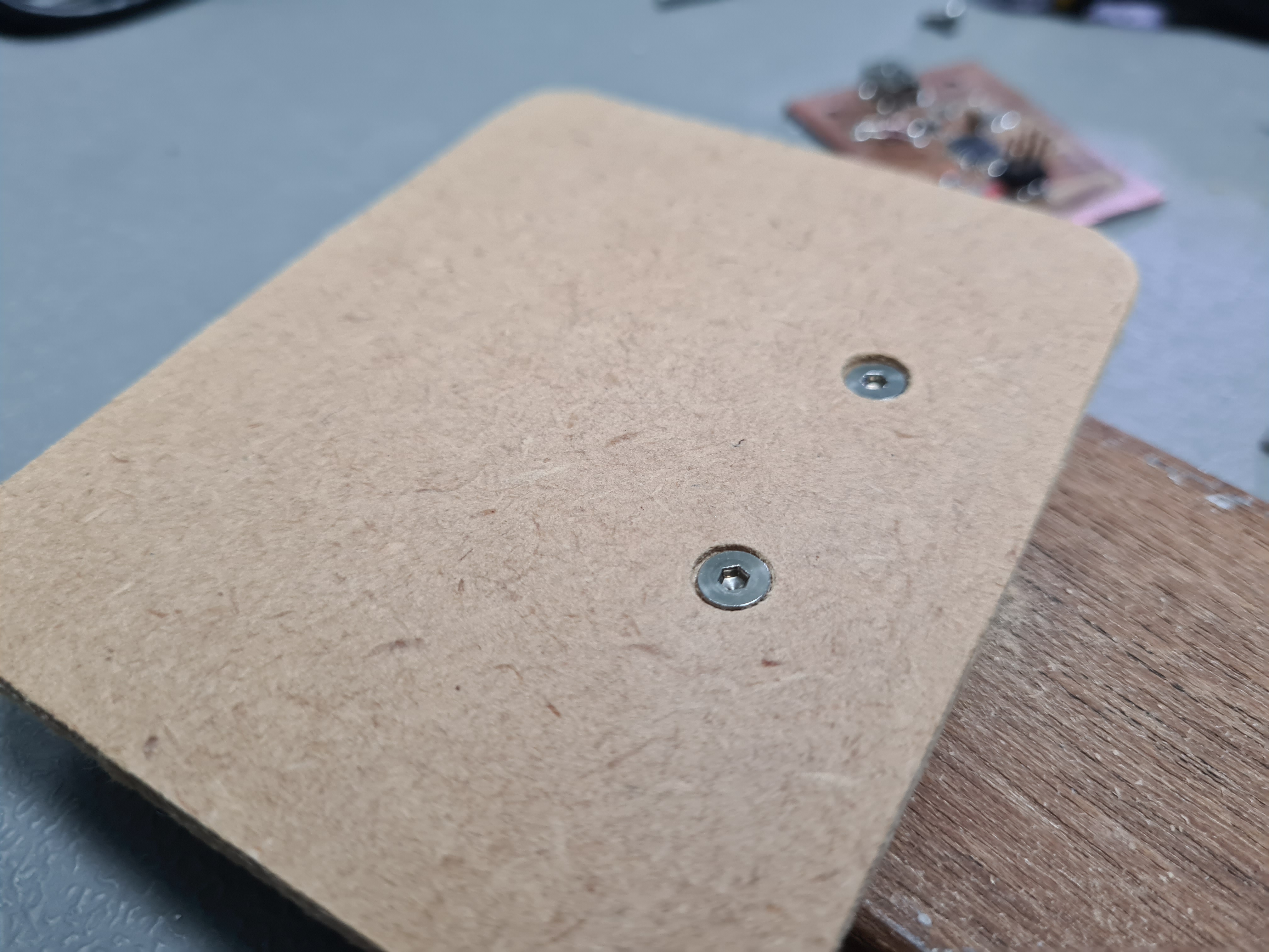
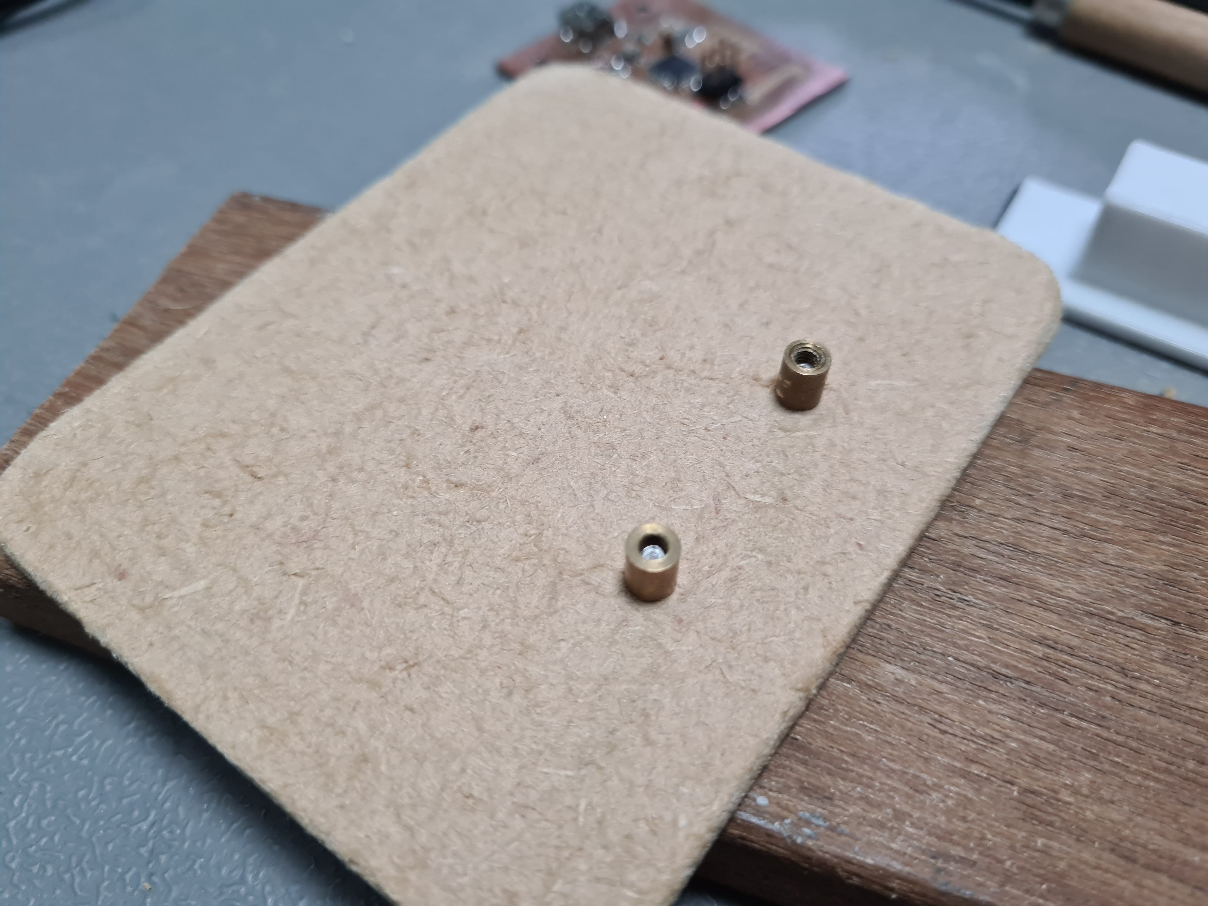
On the inside, the PCB is offset from the bottom using 6mm brass standoffs. The PCB would be screwed upside down into the bottom case using m3x5 regular screws.
Afterwards, I did some more guesstimating for the placement of ISP header and reset button, and made holes for it using a drill and a file.
I then drilled the 4 holes to mount the top plate to in the top piece. After all this hackjobs were done, I glued together the 2 pieces of the bottom case using wood glue, and left it to dry overnight uder a weight.
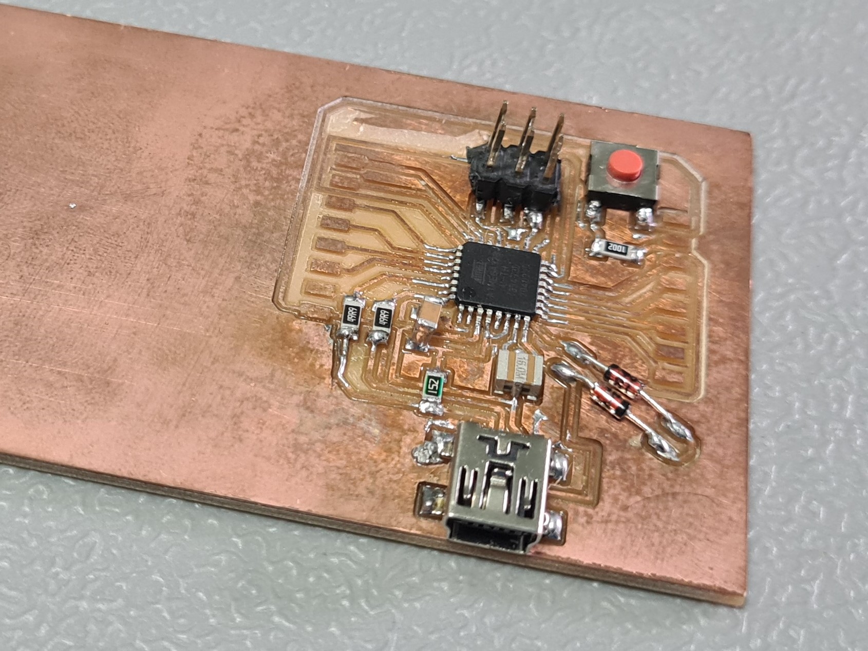
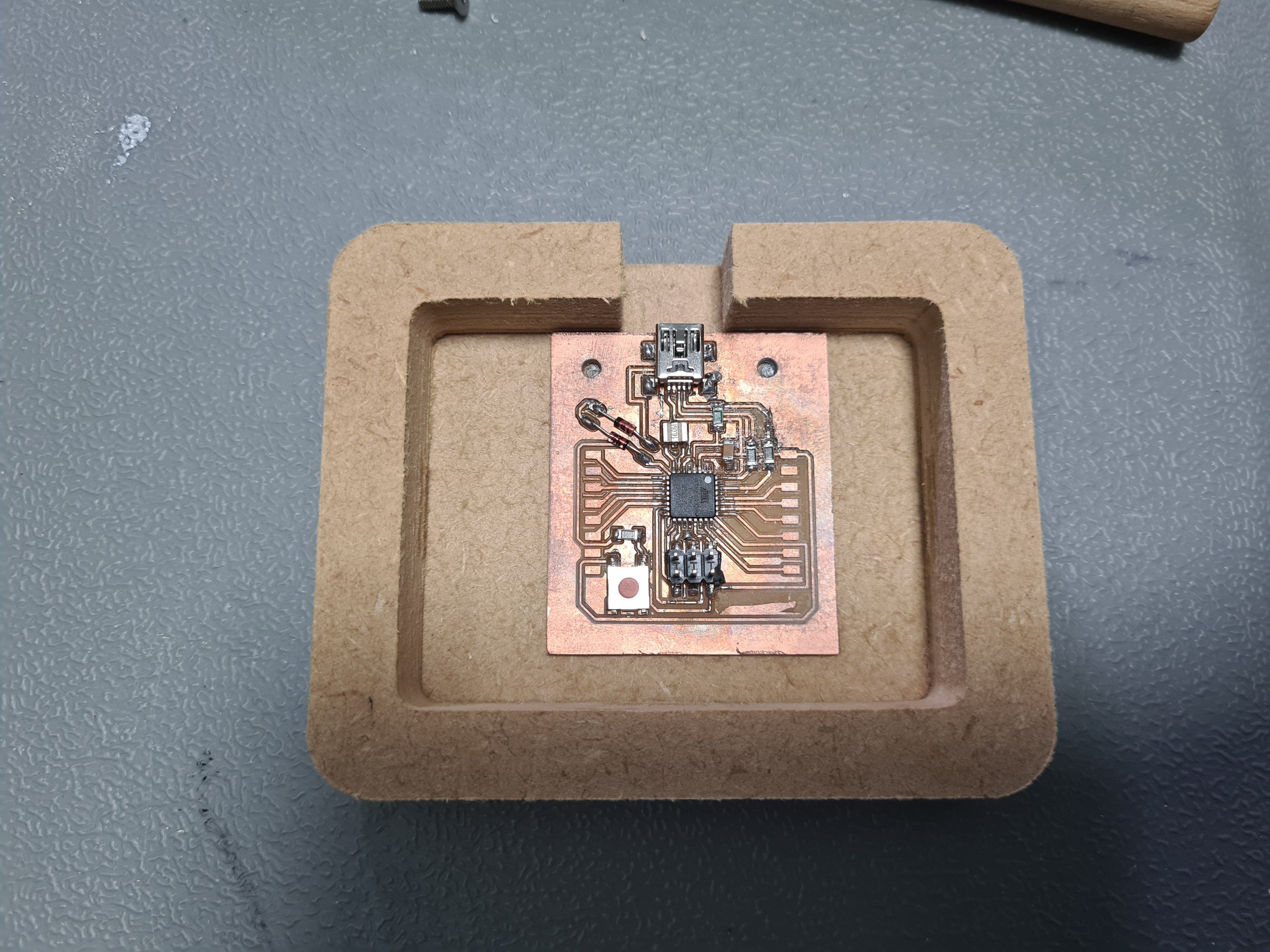
The next day, I test fit the PCB. Here, you can see how the PCB would be mounted using the m3x5 screws. As the screws were still too long, it would not screw tight all the way, which is why theres a 1mm plastic spacer in there.
Once I confirmed that the PCB can fit and both the ISP and miniusb are accessible, I took the pcb off the bottom case. I unscrewed from the countersunk screws and left the standoffs attached to the pcb.
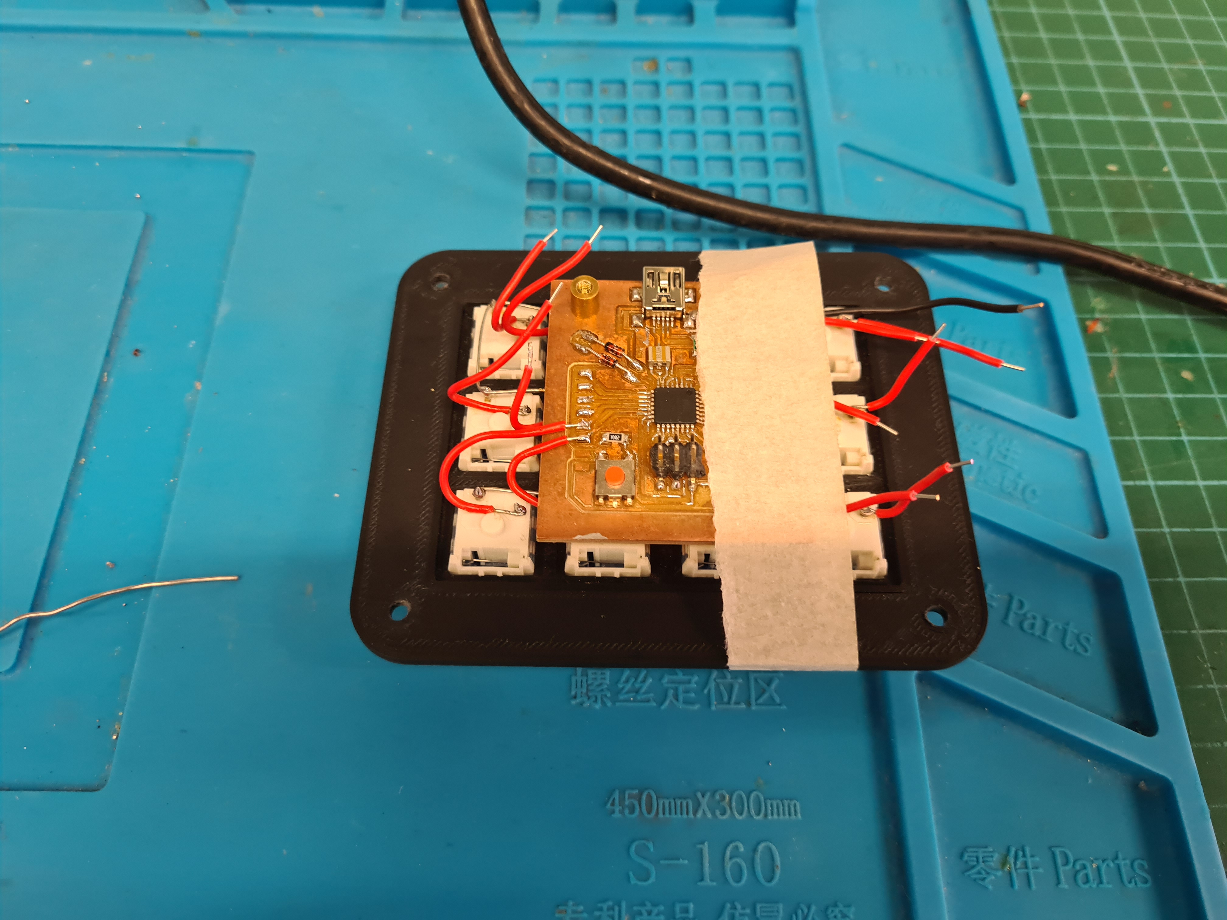
Then, I clicked my mechanical switches into the top plate. Using a stripped single core wire, I ran the wire around one pin of each pin to be ground and snaked through all the switches, ending at the top right where the ground pad of the PCB is.
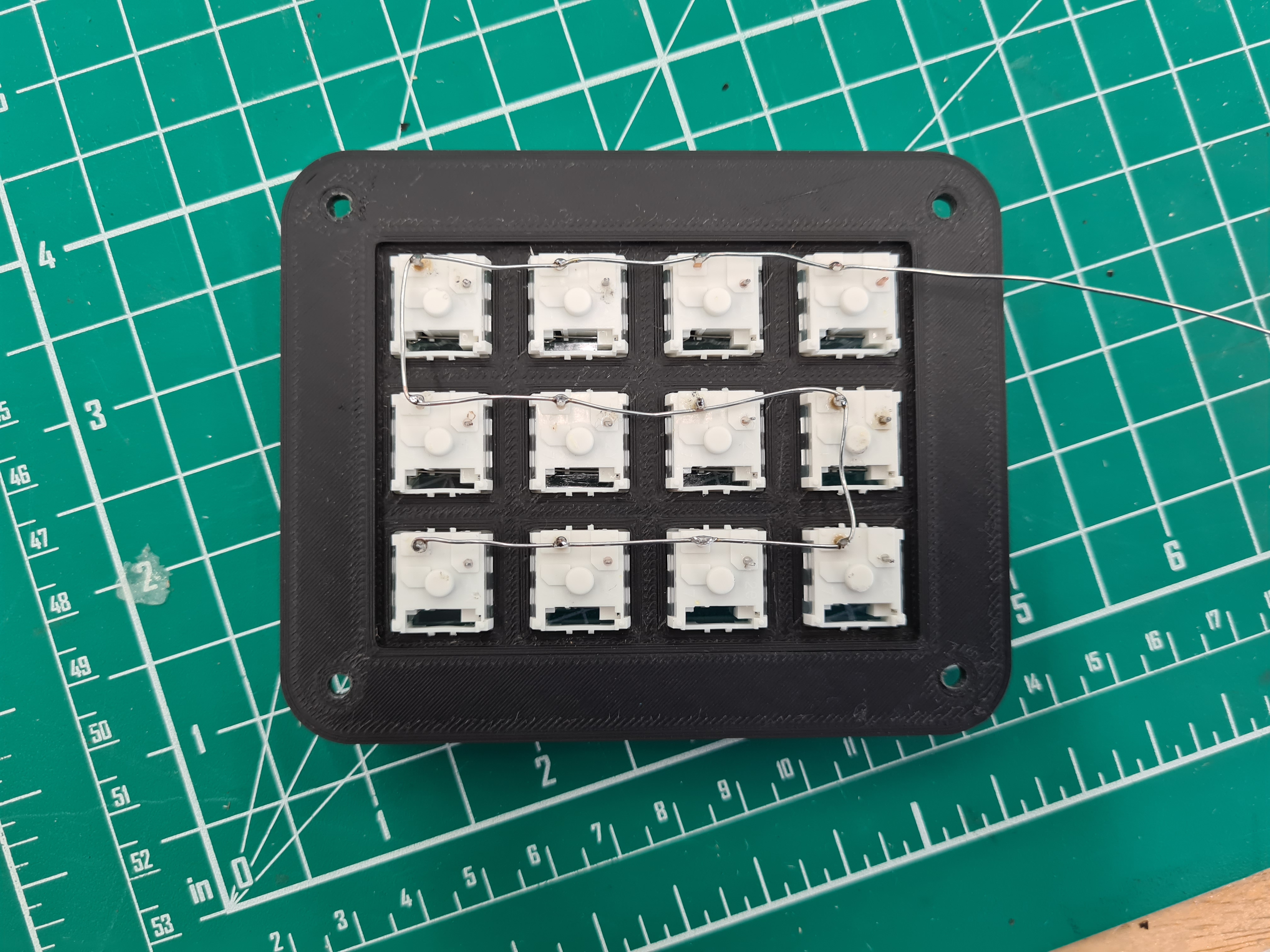
Once that was done and soldered, I made a loop with shorter red wires and placed them on the other pin of the switch.
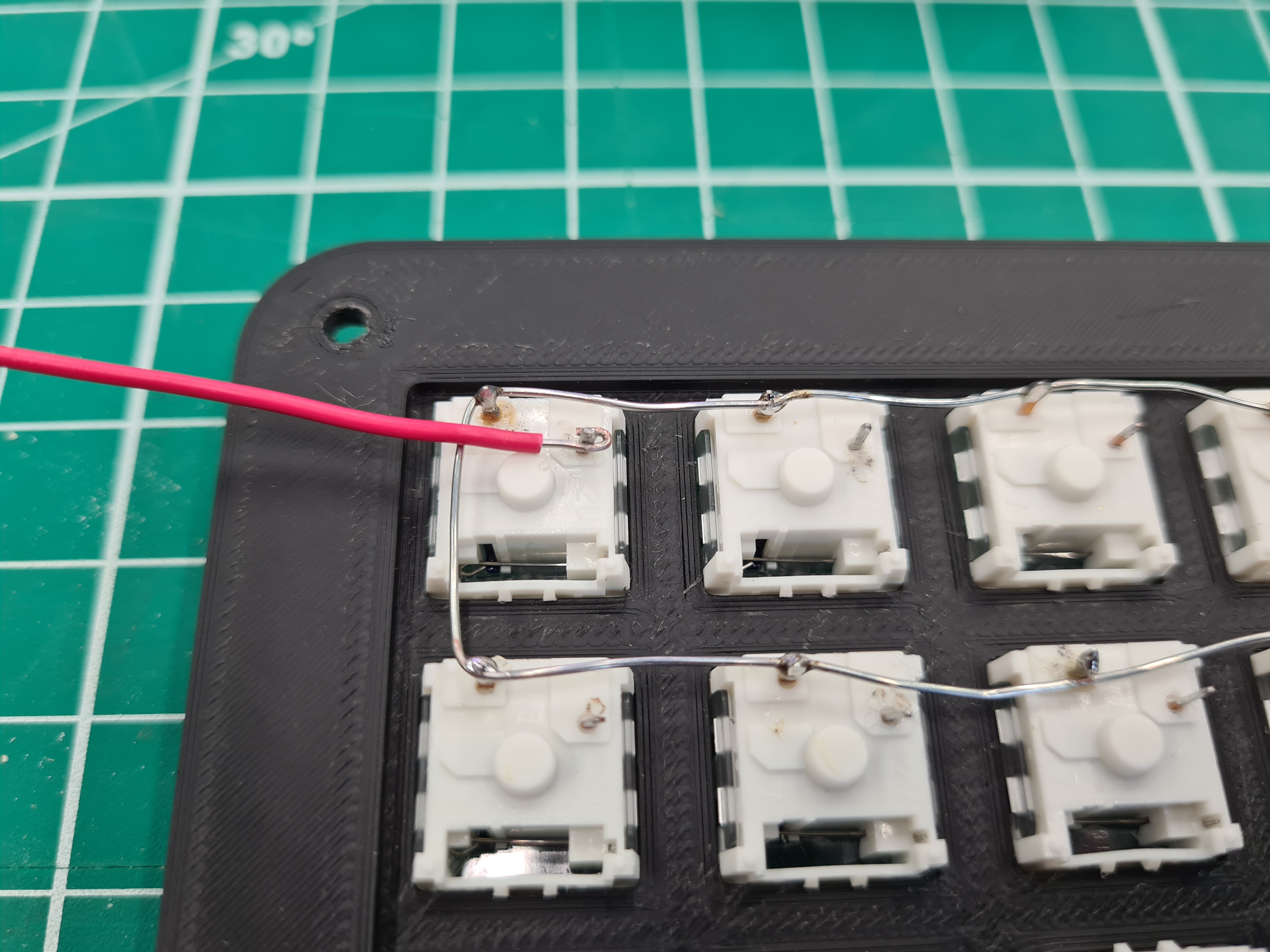
I did so for the remaining switches and soldered all the pins. Every so often, I would check for shorts and if the connections were sound using a multimeter. I made sure that the left 6 switches' wires go to the left and the right 6 right to wrap around the pcb.
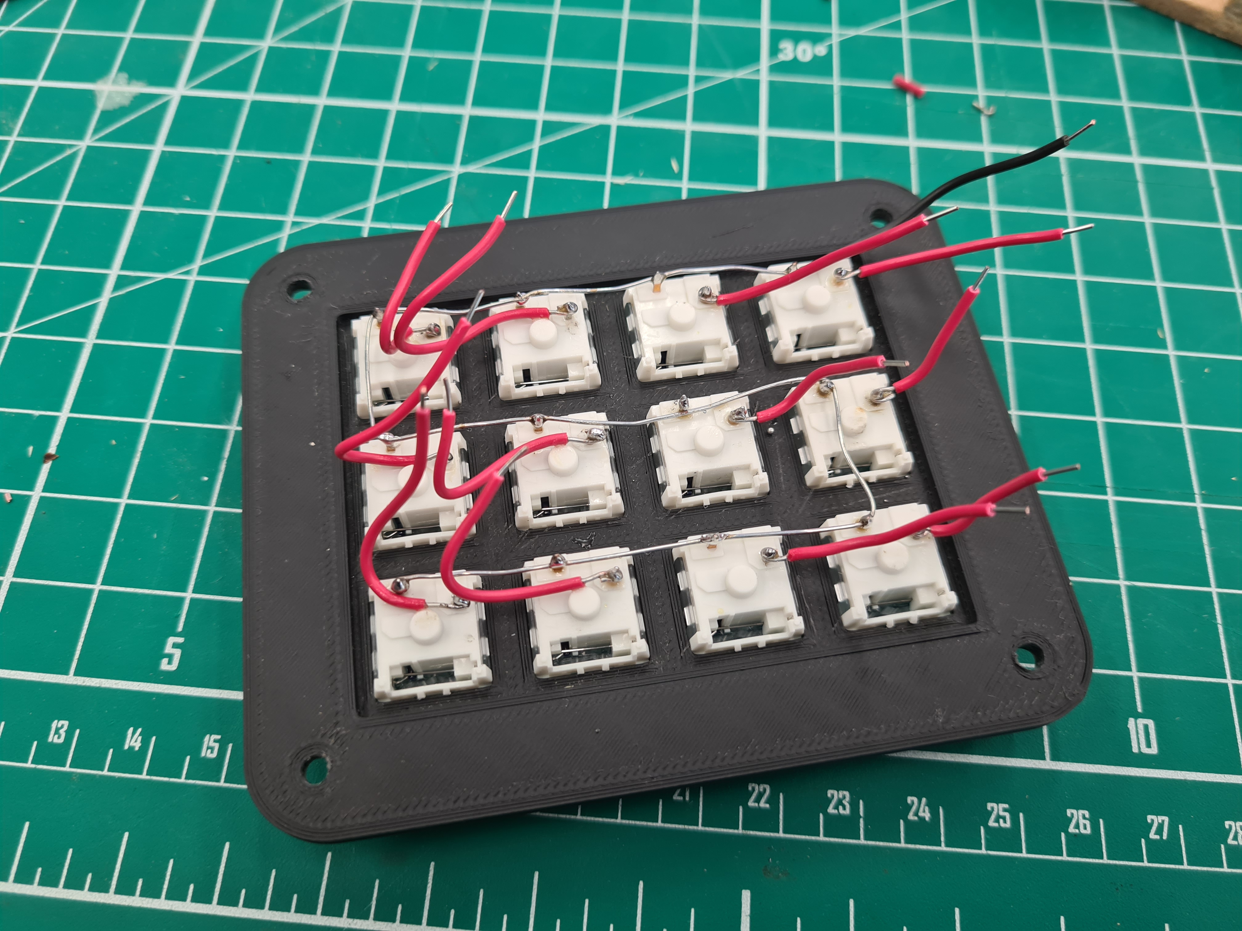
Once all the wires were soldered on the switches, I placed the pcb on top of all the wires. I taped down one side and focused on the soldering the left side.
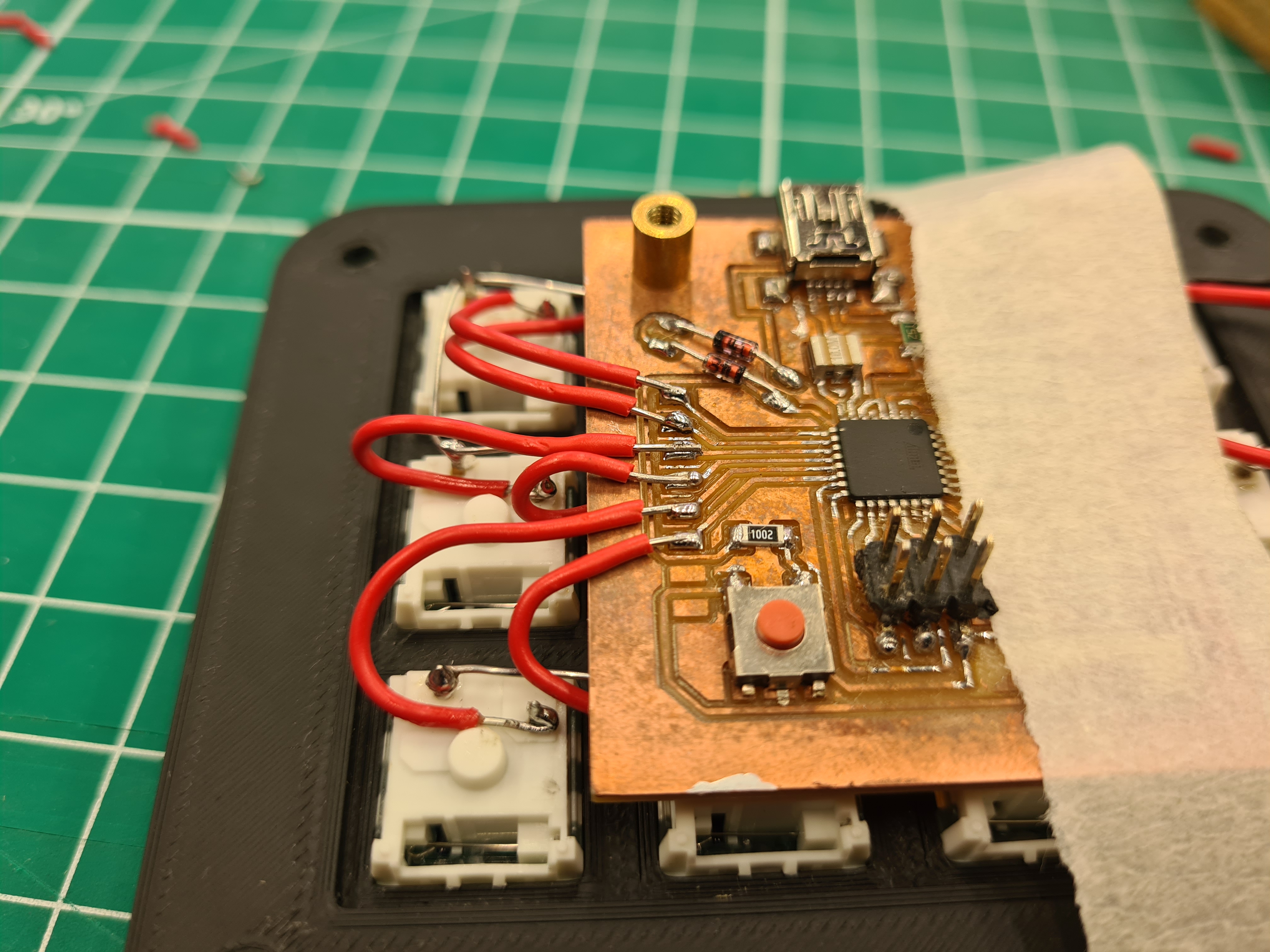
Once the left side was all soldered, I removed the tape and soldered on the right side the same way. At this point, which switch went to which pad did not matter as I can change it in code later on.
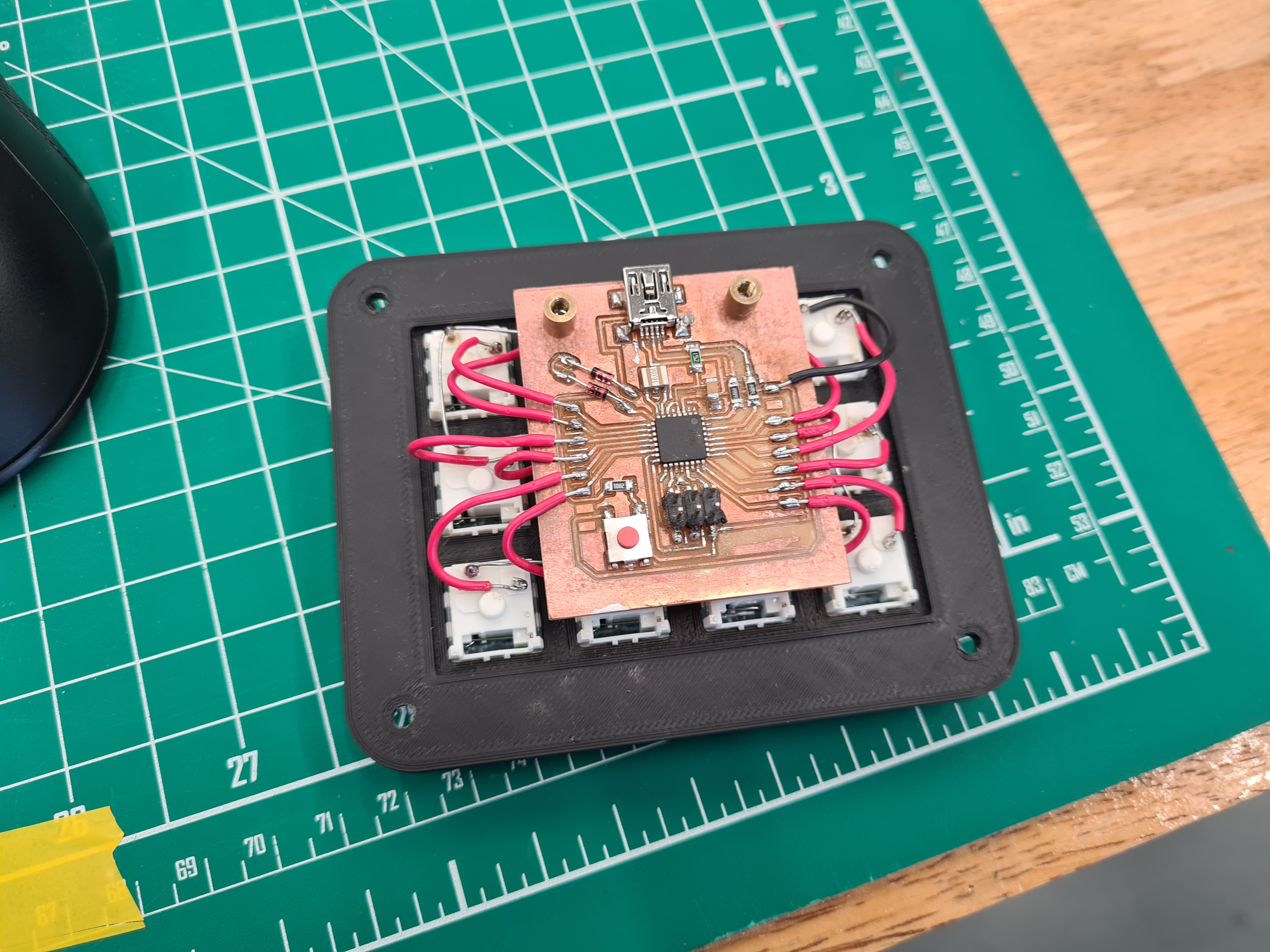
Once that was done, I checked for one final time that all the connections were sound and that there were no shorts. When I was confident that all the connections were good to go, I got the bottom case and screwed everything in. I first lined up the standoffs of the PCB with the bottom case holes and screwed them in. Once that was done, I aligned the 4 top holes and used m3x8 screws to hold it down.
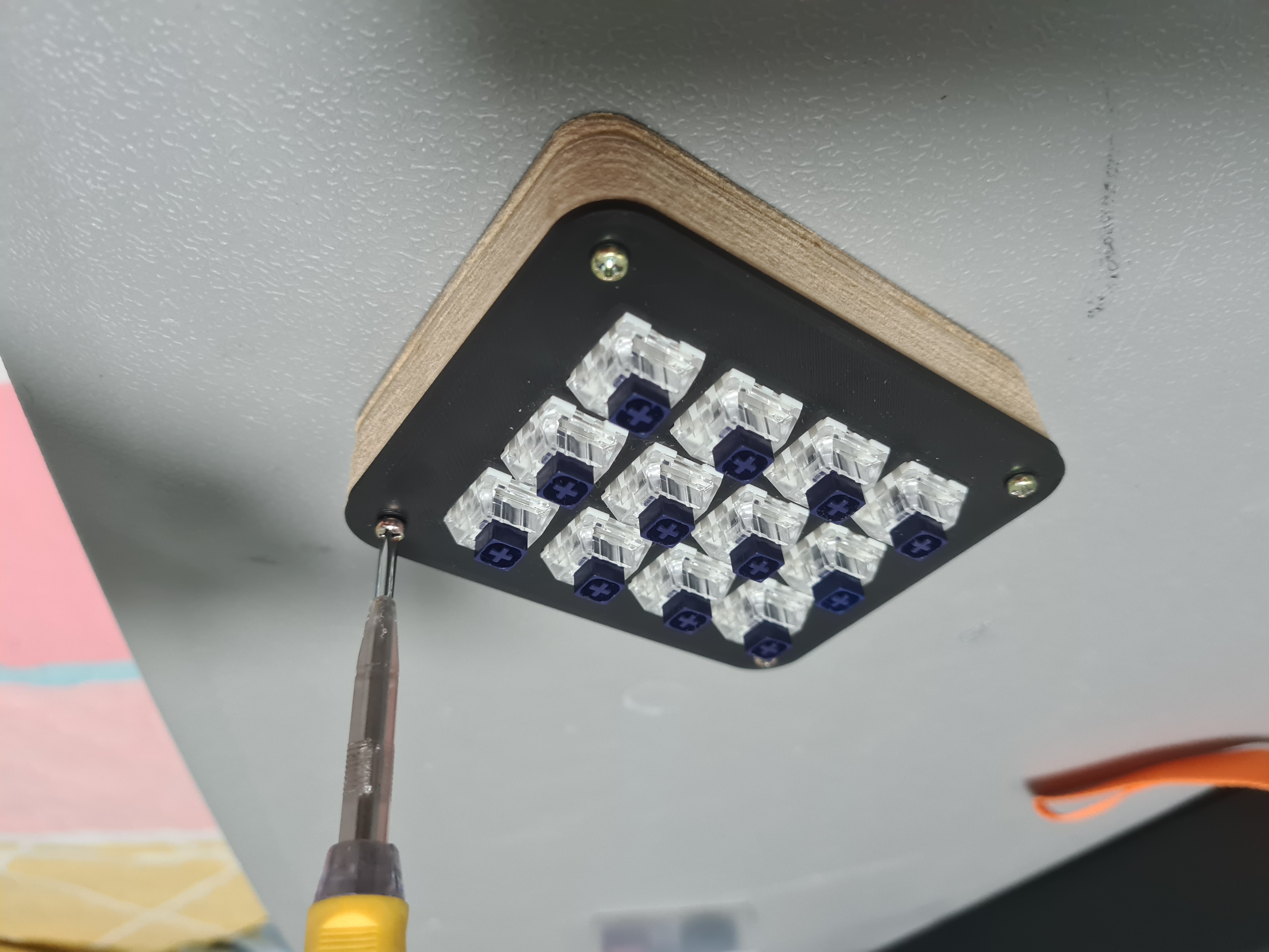
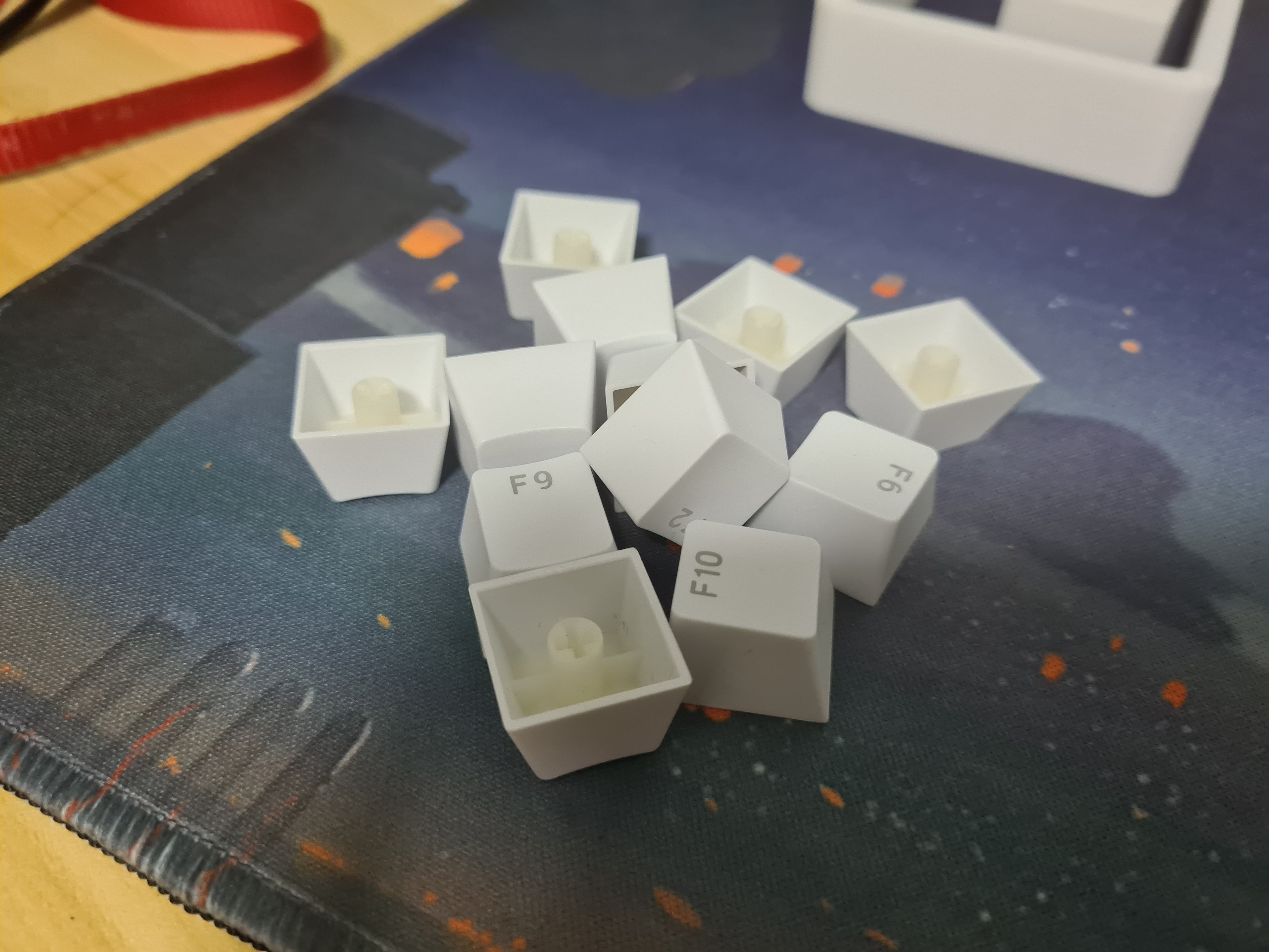
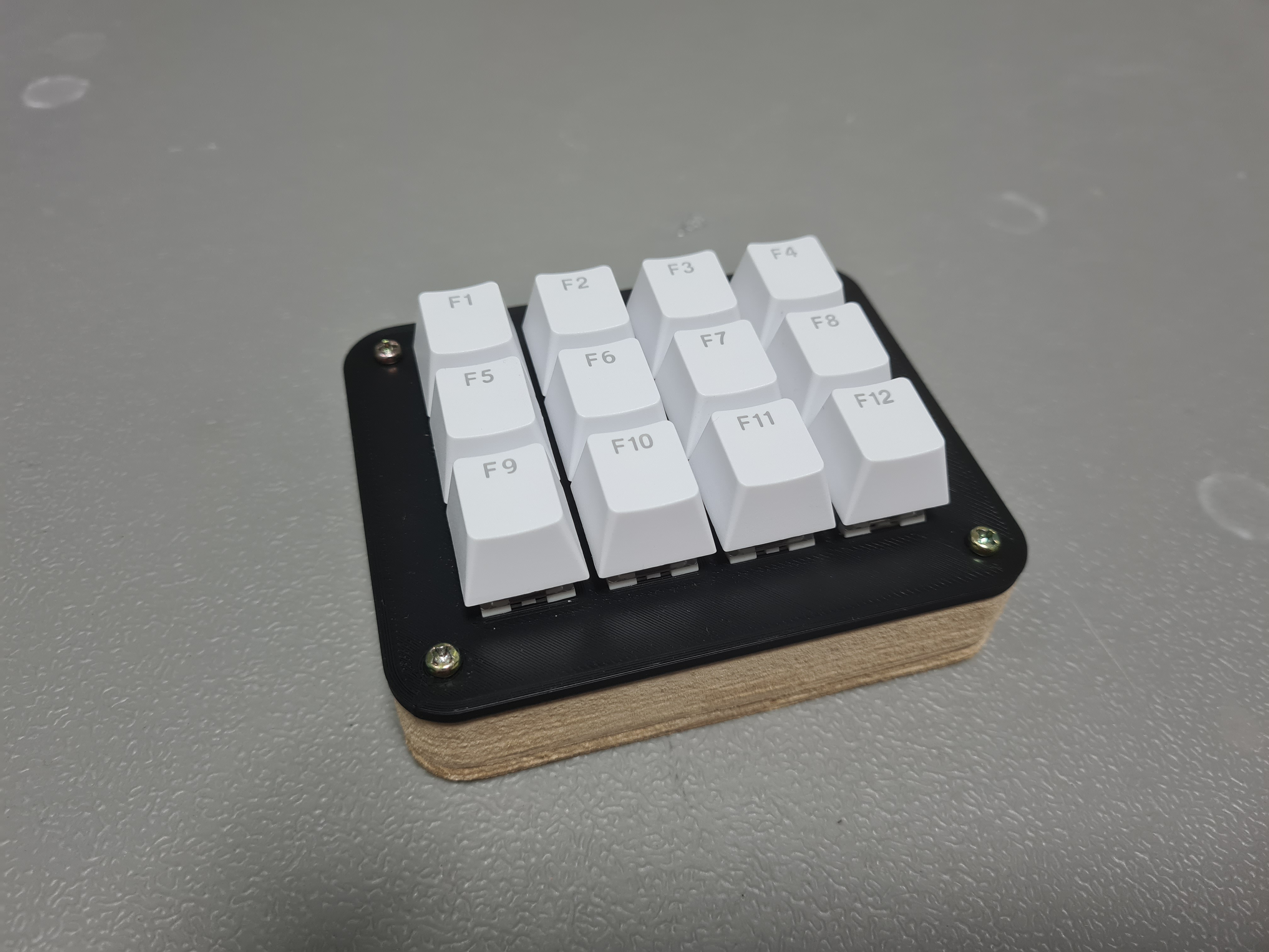
After that was done, I just added some spare F1-F12 keycaps I had lying around to the switches.
And with that, the hardware is all done, now it is time to program the board.
Coding
Initially, I wanted to reference and use the source code from the HIDKeys project, found here. Although the HIDKeys example uses a mega8, I thought, as the atmega328 just has more memory, the same code would still work.
It did not.
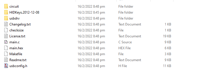
No matter what I did, I could not flash the firmware. Here are the source files of the HIDKeys project.
Zi Hon helped me out and together we spent around 3 hours on it. We tried changing the MCU and programmer in the makefile and made new hex files, we editted the main.c files, changed the set fuses in the makefile. At one point Mr Steven Chew came over to take a look and realised some scripts required a linux machine, so I used git Bash, and tried flashing it there, still did not work.
Even though nothing we tried worked, I still learnt a lot, like what to look out for when flashing firmware onto a chip. I also learnt about fuse settings. Mr Steven Chew directed me to a fuse calculation website where I can check fuses for different chips and what they mean, as well as setting fuses using AVRdude in terminal.
In the end, I decided to scrap using HIDKeys and brought up a v-usb library I found a few days prior. I thought that I would not be able to use the library, as on the documentation it said it required completely different hardware, and it used different D+ and D- pins for the v-usb. Zi Hon then told me that they should be edittable, and taught me how to look for it.
He first just quickly browsed through the utilities of the library and found a few lines that looked important.
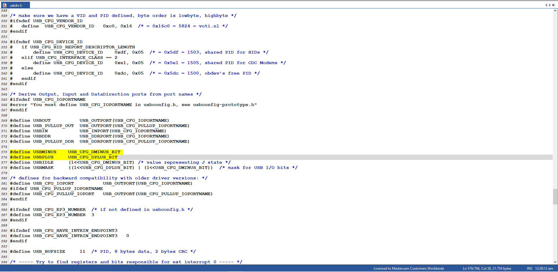
From these 2 lines, he said that they should be defined elsewhere, but we did not know exactly where. So he opened up arduino IDE and editted the preferences. He made it show verbose output during compilation and show all compiler warnings.
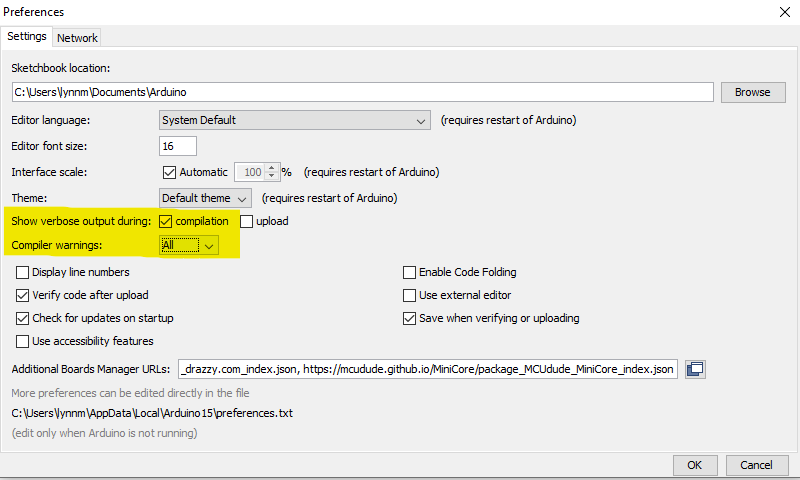
He then opened the example keyboard program from the library and redefined the 2 lines he found. Because in the documentation shows that D+ and D- are 2 and 4 respectively, he just put in any number other than those 2.
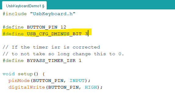
He then verified the code, and arduino IDE would show an error that pinpointed exactly where it was previously defined.
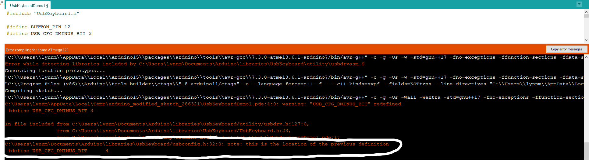
We then navigated to the file location and, sure enough, it was there.
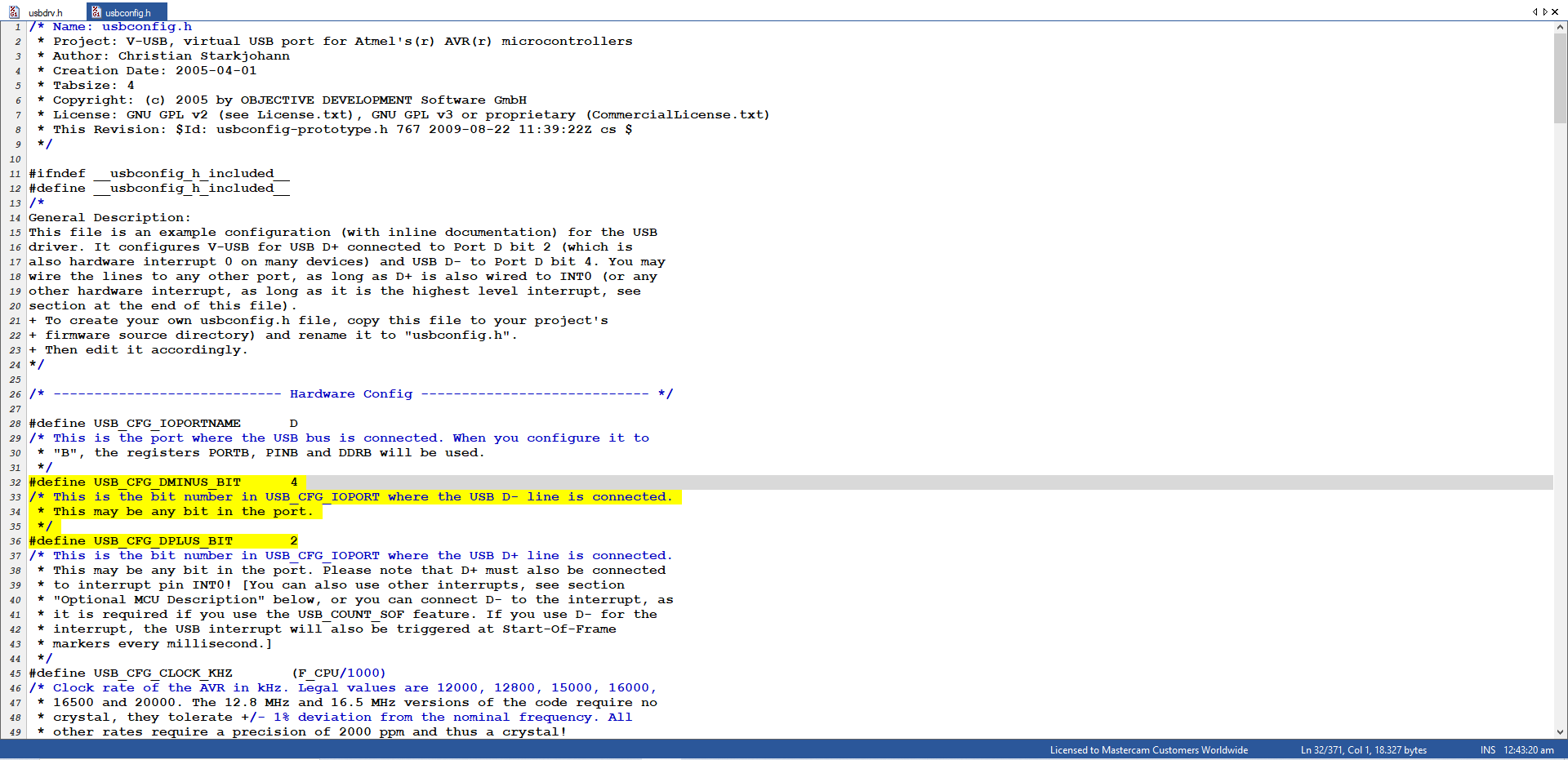
Because HIDKeys used pin 2 as D+ and pin 0 as D-, I just changed the DMINUS_BIT to 0. Once that was done, I saved the file, went back to preferences to turn off all the compiler warning messages, and uploaded the demo program. The program simple inputs a "hello world" followed by enter.
And it worked. I plugged in the mini usb and my laptop immediately recognised it as a USBKeyboard. I did not have photos of this part but when I clicked the keyswitch I set it to, it sent the "hello world" message. Once I got the USB part working, the rest of the code was very, very simple.
I first defined every switch to the corresponding pin. This just took a lot of trial and error to find out the sequence.
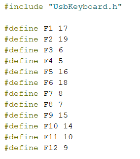
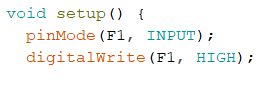
I then setup each switch as a input and wrote a HIGH to it, as the switches are active low. It is just these 2 lines copy pasted 11 more times for F2-F12.
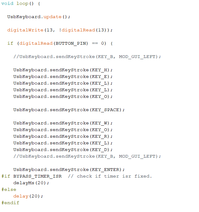
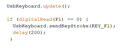
Then, in the loop, I put USBKeyboard.update();, then for each switch to just send the corresponding keystroke.
And with that, the code is done.
Final Result
Here is the final product in action, which is just me pressing it from F1-F12. Here is the website I used to do the keytest.
Here is the 1 minute video I made to showcase the project.
And here is the 1 page slide I made to showcase the project.
Final Thoughts
This was a really fun module, I got to learn many skills and techniques that I would have otherwise missed out. Special thanks to Mr Steven Chew for guiding us through this module, and to Zi Hon for helping me out so much as well.
As for my final project, I still don't how why it even worked to begin with, honestly speaking I think I just got lucky. It was using schematics last updated in 2012 for a different chip, with a library last updated 7 years ago where the hardware does not even match. 2 of my friends tried replicating my project, and even when trying to replicate as best as they can, the computer could not recognise either's PCBs as a keyboard, and I cannot explain why.
In terms of design, there are more to improve as well. In the future, when I revisit this project, I would try to make an integrated PCB, where the switches solder into the PCB, eliminating the need for wires. I would also try to put more thought into the case design, instead of having to resort to manual labor to make it work. Honestly, I am quite dissapointed in what I achieved for the project, I could have done more.
Nevertheless, it is over and done, I tried my best at the time. Thanks for reading up to here, peace.
- final entry, lynn myat moe aung, signing out.